Nickel Silicide Evaporation Materials
Introduction
Nickel Silicide Evaporation Materials are advanced thin film sources used in semiconductor manufacturing, microelectronics, and metallization processes. As a key compound in the nickel–silicon system, nickel silicide (NiSi, Ni₂Si, or NiSi₂ depending on stoichiometry) is prized for its low resistivity, excellent thermal stability, and strong adhesion to silicon substrates. These properties make it an essential evaporation material for forming high-quality silicide layers in integrated circuits, Schottky barriers, and contact metallization.
Detailed Description
Nickel Silicide is a metallic compound formed by reacting nickel and silicon at controlled ratios and high temperatures. The resulting material exhibits metal-like conductivity with good diffusion resistance, ensuring stable electrical contact between metal and semiconductor layers.
Meticulously produced by high-temperature synthesis followed by crushing, purification, and vacuum sintering, Nickel Silicide evaporation materials provide:
Uniform composition: Ensures consistent stoichiometry for reproducible film properties.
High purity (up to 99.9%): Minimizes contamination during vacuum deposition.
Excellent adhesion and stability: Compatible with both silicon wafers and oxide layers.
High melting point (≈ 990–1,330 °C depending on phase): Suitable for thermal and e-beam evaporation systems.
Low resistivity: Enables reliable, ohmic contact formation in semiconductor devices.
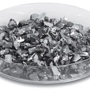
They are typically available in pellets, granules, or pieces for use in thermal boats or electron-beam crucibles. Custom stoichiometry (NiSi, Ni₂Si, NiSi₂) can be tailored to specific deposition needs.
Applications
Nickel Silicide evaporation materials are widely used across advanced technology sectors:
Semiconductor manufacturing: Formation of self-aligned silicide (salicide) contacts in CMOS processes.
Microelectronics: Metal interconnects, diffusion barriers, and Schottky junctions.
Thin film resistors and contacts: Low-resistivity coatings on silicon and polysilicon.
Optical and decorative coatings: Metallic films requiring good reflectivity and durability.
Research & development: Used in thin film studies for nanoelectronics and material science.
Technical Parameters
| Parameter | Typical Value / Range | Importance |
|---|---|---|
| Chemical Formula | NiSi, Ni₂Si, or NiSi₂ | Different phases affect conductivity and thermal stability |
| Purity | 99.5% – 99.9% | Higher purity ensures low impurity diffusion |
| Density | 6.3 – 6.7 g/cm³ | Affects film growth rate and uniformity |
| Melting Point | 990 – 1,330 °C | Suitable for e-beam and thermal evaporation |
| Resistivity | 10–20 µΩ·cm | Enables low-resistance electrical contacts |
| Evaporation Method | Thermal / Electron-beam | Determines film quality and deposition rate |
| Particle Size | 3 – 6 mm (custom) | Ideal for stable evaporation rate |
Comparison with Related Materials
| Material | Key Advantage | Typical Application |
|---|---|---|
| Nickel Silicide (NiSi) | Low resistivity, excellent adhesion | Semiconductor contact layers |
| Titanium Silicide (TiSi₂) | Higher temperature stability | High-speed transistor contacts |
| Cobalt Silicide (CoSi₂) | Good uniformity on narrow lines | Advanced CMOS devices |
FAQ
| Question | Answer |
|---|---|
| Which nickel silicide phase should I choose? | NiSi is most common for low-resistance contacts, while Ni₂Si and NiSi₂ are used for specific temperature and resistivity requirements. |
| Can the product be customized? | Yes. Purity, stoichiometry, shape, and packaging can be tailored according to your deposition system. |
| What evaporation systems are compatible? | Suitable for both electron-beam and thermal evaporation systems under high vacuum. |
| Is it stable in air? | Nickel silicide is relatively stable but should be stored in a vacuum-sealed or inert-gas-filled container to prevent surface oxidation. |
| How is it packaged for shipment? | Each batch is vacuum-sealed, labeled with full traceability information, and cushioned in export-safe cartons or wooden crates. |
| Which industries commonly use it? | Semiconductor, microelectronics, optoelectronics, and R&D laboratories. |
Packaging
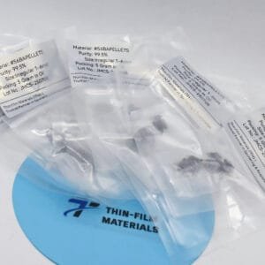
Our Nickel Silicide Evaporation Materials are carefully sealed under vacuum or inert gas to prevent oxidation. Each container is labeled with material name, composition, purity, batch number, and net weight. Protective foam and double-layer export packaging ensure safe transportation and long-term storage stability.
Conclusion
Nickel Silicide Evaporation Materials combine excellent electrical performance with strong thermal and chemical stability, making them a preferred choice for modern semiconductor and microelectronic thin film processes. Whether for contact formation, metallization, or barrier layers, NiSi-based materials deliver reliable and consistent film properties under demanding deposition conditions.
For detailed specifications and quotations, please contact us at [sales@thinfilmmaterials.com].


 MSDS File


Reviews
There are no reviews yet.