
 MSDS File
Product Overview
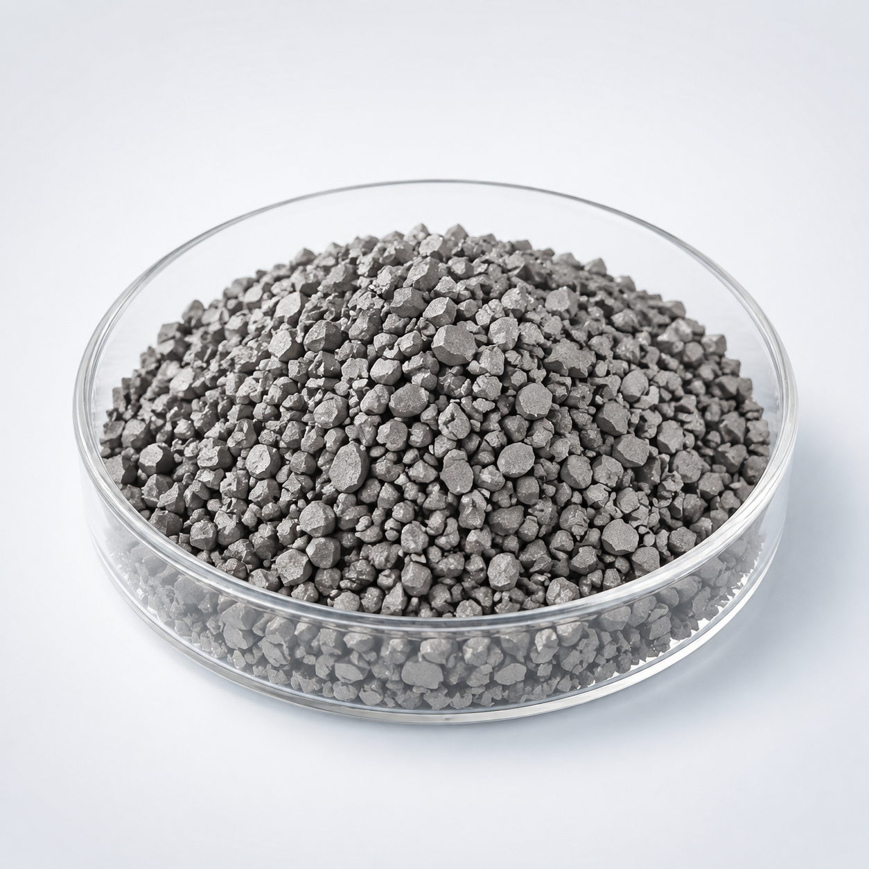
Nickel Silicide Evaporation Materials (NiSi2) is a high-melting compound evaporation source for specialized thin-film deposition and materials research. Carbides, borides, nitrides, silicides, and related compounds may require electron-beam heating or other high-energy evaporation methods, and some compounds can decompose or change composition before a useful vapor pressure is reached. The evaporation route should therefore be qualified against the required film chemistry rather than assumed to be congruent.
Evaporation Behavior and Process Considerations
These compounds commonly require high-energy evaporation methods such as electron-beam heating. However, high source temperature can also promote decomposition, dissociation, or preferential evaporation. Process qualification should therefore include source-behavior observation and film-composition verification before scaling to long runs.
Technical Data
| Parameter | Typical Value / Range | Importance |
|---|---|---|
| Chemical Formula | NiSi₂ | Determines compound stoichiometry |
| Purity | 99.9% – 99.99% | Ensures stable electrical properties |
| Form | Pellets / Granules / Tablets / Pieces | Compatible with evaporation systems |
| Particle Size | 1 – 6 mm typical | Supports uniform evaporation |
| Deposition Method | Thermal evaporation / E-beam evaporation | Suitable for PVD thin film processes |
| Density | High-density compound material | Ensures stable evaporation behavior |
| Material | Key Advantage | Typical Application |
|---|---|---|
| Nickel Silicide (NiSi₂) | Low resistivity and strong silicon compatibility | Semiconductor contacts and interconnects |
| Nickel (Ni) | High conductivity and good adhesion | Metallization layers |
| Titanium Silicide (TiSi₂) | Very low resistivity for high-speed devices | Semiconductor contacts |
| Question | Answer |
|---|---|
| What deposition methods are suitable for NiSi₂ evaporation materials? | NiSi₂ materials are commonly used in thermal evaporation and electron beam evaporation systems. |
| What forms are available for evaporation materials? | Typical forms include pellets, granules, tablets, rods, or custom pieces. |
| Why is nickel silicide used in semiconductor devices? | Nickel silicide provides low-resistance electrical contacts and excellent compatibility with silicon. |
| Can the material composition be customized? | Yes. Different nickel silicide phases or compositions can be produced depending on application requirements. |
| What substrates can NiSi₂ films be deposited on? | NiSi₂ films are commonly deposited on silicon wafers and other semiconductor substrates. |
Typical Thin-Film Applications
- Hard, refractory, electronic, protective, and specialty compound thin films
- High-temperature or advanced-material coating research
- R&D evaluating decomposition behavior and film stoichiometry under e-beam evaporation
Source Form and Ordering Considerations
For quotation, provide the material or formula, purity, desired source form and size, quantity, evaporation method if known, and any crucible, boat, or e-beam hearth constraints. For compound materials, include the target film composition or application when possible so that source form and process risk can be reviewed together. TFM can supply pellets, pieces, granules, tablets, or other custom forms subject to material manufacturability.
Frequently Asked Questions
Can Nickel Silicide be evaporated by electron beam?
Electron-beam heating is often evaluated for high-melting compounds because it can provide localized high temperature. However, the compound may decompose before evaporating congruently.
Will Nickel Silicide maintain its stoichiometry during evaporation?
Not necessarily. Carbides, borides, nitrides, silicides, and related compounds can dissociate or evaporate preferentially, so film composition should be verified.
Why is source conditioning important for Nickel Silicide?
Gradual conditioning reduces thermal shock, outgassing, and sudden particle ejection while allowing the operator to observe whether the compound remains stable under heating.
What source holder should be used for Nickel Silicide?
The holder must tolerate the required temperature and avoid chemical reaction with the charge. E-beam hearth or compatible crucible selection should be reviewed for the specific material.
Is a pellet or dense piece preferable for Nickel Silicide?
A dense, mechanically stable charge is generally easier to load and condition than loose powder. The ideal form depends on hearth size and the required evaporation rate.
What information should I provide for a Nickel Silicide evaporation-material quotation?
Provide formula, purity, source form, piece or pellet size, quantity, evaporation method, source-holder details, and the intended film composition or application.
Reviews
There are no reviews yet.