 MSDS File
Introduction
Nickel Telluride (NiTe) Evaporation Materials are compound semiconductor sources used in physical vapor deposition (PVD) for producing nickel–tellurium thin films with controlled composition and functional electronic properties. As a transition-metal telluride, NiTe is of growing interest in optoelectronics, thermoelectric research, and phase-change or functional chalcogenide systems where precise stoichiometry and film uniformity are essential.
Detailed Description
NiTe evaporation materials are synthesized from high-purity nickel and tellurium with strict stoichiometric control to ensure a stable Ni:Te ratio. Advanced synthesis and consolidation processes are employed to minimize impurities, reduce volatile loss, and improve evaporation stability under high vacuum.
Nickel telluride can be deposited using thermal evaporation or electron-beam evaporation, depending on system configuration and desired deposition rate. Careful control of source temperature and evaporation rate helps maintain film composition and surface smoothness. Compared with depositing nickel and tellurium separately, using a compound NiTe evaporation source simplifies process control and improves batch-to-batch reproducibility.
NiTe thin films exhibit tunable electrical conductivity, good adhesion to common substrates, and compatibility with multilayer chalcogenide stacks. These characteristics make NiTe evaporation materials suitable for both exploratory research and prototype device fabrication.
Applications
Nickel Telluride evaporation materials are commonly used in:
Chalcogenide thin films: Functional Ni–Te layers and compound semiconductors
Thermoelectric research: Nickel-based telluride materials and heterostructures
Optoelectronics: Functional layers in photonic and electronic devices
Phase-change and functional materials: Research on telluride-based systems
Thin-film sensors: Electrically responsive coatings
Academic & industrial R&D: Materials science and device development
Technical Parameters
| Parameter | Typical Value / Range | Importance |
|---|---|---|
| Chemical Composition | NiTe (Nickel Telluride) | Defines electrical & structural properties |
| Purity | 99.9% – 99.99% | Reduces defects and contamination |
| Stoichiometry | Ni:Te ≈ 1:1 | Ensures consistent film behavior |
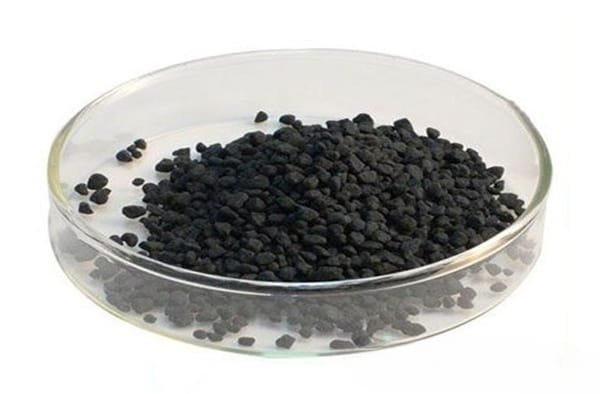
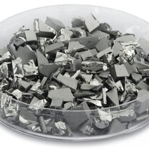
| Form | Pieces, pellets, granules | Compatible with evaporation sources |
| Evaporation Method | Thermal / E-beam | Flexible PVD integration |
| Application Type | Thin-film deposition | Semiconductor & functional coatings |
Comparison with Related Telluride Materials
| Material | Key Advantage | Typical Application |
|---|---|---|
| NiTe | Stable Ni–Te compound, tunable conductivity | Functional telluride films |
| Bi₂Te₃ | High thermoelectric performance | Thermoelectric devices |
| Sb₂Te₃ | Phase-change functionality | Memory & optics |
| CdTe | Direct bandgap semiconductor | Photovoltaics |
FAQ
| Question | Answer |
|---|---|
| Can NiTe evaporation materials be customized? | Yes, purity, form, and batch size can be tailored. |
| Which evaporation method is recommended? | Both thermal and electron-beam evaporation are commonly used. |
| Is stoichiometry stable during evaporation? | Controlled evaporation parameters help maintain Ni:Te balance. |
| How are the materials packaged? | Vacuum-sealed with moisture- and contamination-resistant protection. |
Packaging
Our Nickel Telluride Evaporation Materials (NiTe) are meticulously tagged and labeled externally to ensure efficient identification and strict quality control. Each batch is vacuum-sealed and protected with reinforced cushioning to prevent oxidation, tellurium loss, or mechanical damage during storage and transportation.
Conclusion
Nickel Telluride Evaporation Materials (NiTe) provide a reliable and controllable source for depositing nickel–tellurium thin films with consistent composition and functional performance. With flexible evaporation formats, stable material quality, and customization options, NiTe is well suited for advanced research and emerging chalcogenide thin-film applications.
For detailed specifications and a quotation, please contact us at sales@thinfilmmaterials.com.


Reviews
There are no reviews yet.