Generic selectors
Exact matches only
Search in title
Search in content
Post Type Selectors

VD0566 Niobium Evaporation Materials, Nb

Material Type: Niobium
Symbol: Nb
Purity: 99.9% ~ 99.99%
Shape: Powder/ Granule/ Custom-made

As a leading manufacturer and supplier, TFM specializes in high-purity niobium evaporation materials and a wide array of other evaporation products. We offer these materials in both powder and granule forms, with customization options to cater to your specific requirements.

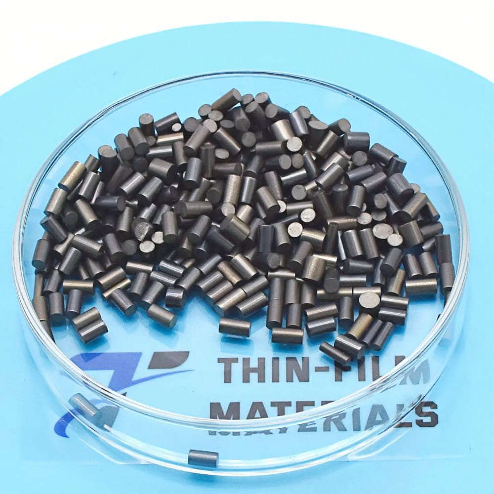
Niobium Evaporation Material Description

Niobium is a light grey, crystalline, and ductile transition metal, particularly noted for its superior ductility in high-purity forms. Its strong resistance to oxidation makes it a preferred hypoallergenic alternative to nickel in jewelry. Additionally, niobium’s low capture cross-section for thermal neutrons makes it valuable in the nuclear sector. Because niobium and titanium share similar physical and chemical properties, they can be challenging to distinguish.

For deposition processes, high-purity niobium evaporation materials are essential to produce high-quality films. TFM specializes in niobium evaporation materials with purities up to 99.99%, ensuring consistent product quality through rigorous quality assurance practices.

niobium evaporation materials

Niobium Evaporation Material Specification

Material TypeNiobium
SymbolNb
Atomic Number41
Color/AppearanceGray, Metallic
Melting Point2,468 °C
Density8.57 g/cc
SynonymsNb Pellets, Nb Pieces, Nb Evaporation Pellet, Niobium Pellets, Niobium Pieces, Niobium Evaporation Pellet

Niobium Evaporation Material Application

Used across a range of deposition techniques like semiconductor deposition, chemical vapor deposition (CVD), and physical vapor deposition (PVD), these processes are essential in various industrial applications. In the field of optics, these methods are employed for several purposes, including enhancing wear resistance, creating aesthetic coatings, and developing advanced display technologies.


Niobium Evaporation Material Packaging

We take great care in managing our niobium evaporation materials, focusing on meticulous handling to prevent any damage throughout storage and transportation. This attention to detail ensures that the materials retain their original quality and condition.

Get Contact

TFM provides a diverse selection of niobium evaporation materials, available in various forms, purities, sizes, and price points to meet different requirements. We specialize in high-purity e-beam evaporation materials, crafted to offer exceptional density and minimal average grain sizes. For the latest pricing on our evaporation pellets or other deposition materials not featured, please reach out to us with your specific inquiry.

Reviews

There are no reviews yet.

Be the first to review “VD0566 Niobium Evaporation Materials, Nb”

Your email address will not be published. Required fields are marked *

FAQ

  • They are high‐purity substances (e.g. metals, alloys, or compounds) used in thermal or electron‐beam evaporation processes to form thin films on substrates.

  • Typically, they’re processed into a form (often ingots, pellets, or wires) that can be efficiently vaporized. Preparation emphasizes high purity and controlled composition to ensure film quality.

  • Thermal evaporation and electron-beam (e-beam) evaporation are the two main techniques, where material is heated (or bombarded with electrons) until it vaporizes and then condenses on the substrate.

  • Thermal evaporation heats the material directly (often using a resistive heater), while e-beam evaporation uses a focused electron beam to locally heat and vaporize the source material—each method offering different control and energy efficiency.

  • Key parameters include source temperature, vacuum level, deposition rate, substrate temperature, and the distance between the source and the substrate. These factors influence film uniformity, adhesion, and microstructure.

  • Evaporation generally produces high-purity films with excellent control over thickness, and it is especially suitable for materials with relatively low melting points or high vapor pressures.

  • Challenges include issues with step coverage (due to line-of-sight deposition), shadowing effects on complex topographies, and possible re-evaporation of material from the substrate if temperature isn’t properly controlled.

  • Common evaporation materials include noble metals (e.g., gold, silver), semiconductors (e.g., silicon, germanium), metal oxides, and organic compounds—each chosen for its specific optical, electrical, or mechanical properties.

  • Selection depends on desired film properties (conductivity, optical transparency, adhesion), compatibility with the evaporation process, and the final device application (semiconductor, optical coating, etc.).

  • Optimizing substrate temperature, deposition rate, and chamber vacuum are critical for ensuring that the film adheres well and forms the intended microstructure without defects.

  • Troubleshooting may involve checking the source material’s purity, ensuring stable source temperature, verifying the vacuum level, adjusting the substrate’s position or temperature, and monitoring deposition rate fluctuations.

While evaporation tends to yield very high purity films with excellent thickness control, it is limited by its line-of-sight nature. In contrast, sputtering can deposit films more uniformly on complex surfaces and is more versatile for a broader range of materials.


Shopping Cart
Scroll to Top