
Introduction
Planar Copper (Cu) Sputtering Target is one of the most widely used materials in physical vapor deposition (PVD) processes. Known for its outstanding electrical and thermal conductivity, copper thin films are essential in semiconductor interconnects, microelectronics, photovoltaic devices, and decorative coatings. Planar Cu targets provide stable sputtering performance and high deposition efficiency in both research-scale and large-area industrial coating systems.
Detailed Description
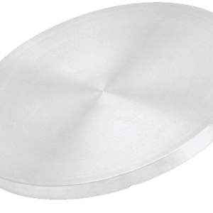
Our Planar Copper Sputtering Targets are manufactured from high-purity copper using vacuum melting, hot working, and precision machining processes to ensure uniform grain structure and minimal impurity levels. Careful control of oxygen and metallic contaminants is critical, as even trace impurities can significantly impact electrical conductivity and film adhesion.
The planar configuration ensures uniform erosion and consistent deposition rates across the substrate surface. High-density targets with homogeneous microstructure reduce arcing and particle generation, enabling stable plasma conditions during DC sputtering. For high-power applications, copper targets can be indium-bonded or diffusion-bonded to copper backing plates to improve heat dissipation and extend target life.
Targets are available in circular, rectangular, and custom planar geometries to match various sputtering cathodes and deposition systems.
Applications
Planar Copper (Cu) Sputtering Targets are widely used in:
Semiconductor interconnect metallization
Printed circuit boards (PCB) and microelectronics
Solar cell and photovoltaic thin films
Decorative and reflective coatings
Barrier and seed layers in multilayer structures
Research and development of conductive thin films
Technical Parameters
| Parameter | Typical Value / Range | Importance |
|---|---|---|
| Material | Copper (Cu) | High electrical conductivity |
| Purity | 99.9% – 99.999% | Minimizes film defects |
| Shape | Planar (round / rectangular) | Uniform deposition profile |
| Thickness | 3 – 15 mm (custom available) | Influences target lifetime |
| Density | ≥ 99.9% theoretical | Improves sputtering stability |
| Sputtering Mode | DC / RF sputtering | Compatible with conductive metal |
| Bonding | Unbonded / Cu backing (optional) | Enhances heat management |
Comparison with Related Materials
| Material | Key Advantage | Typical Application |
|---|---|---|
| Copper (Cu) | Excellent conductivity | Interconnects & electrodes |
| Aluminum (Al) | Lightweight & cost-effective | General metallization |
| Silver (Ag) | Highest conductivity | Reflective & high-end electronics |
| Copper Alloy (Cu/Cr, Cu/Zr) | Improved strength | Wear-resistant coatings |
FAQ
| Question | Answer |
|---|---|
| Is DC sputtering suitable for copper? | Yes, copper is highly conductive and ideal for DC sputtering. |
| Can high-purity grades be supplied? | Yes, purity levels up to 5N (99.999%) are available. |
| Are bonded targets available? | Yes, copper targets can be bonded to backing plates for improved thermal stability. |
| How is the target packaged? | Vacuum-sealed with protective foam and export-grade cartons or wooden crates. |
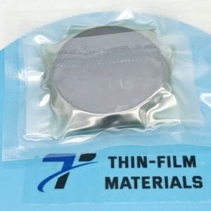
Packaging
Our Planar Copper (Cu) Sputtering Targets are meticulously tagged and labeled externally to ensure efficient identification and strict quality control. We take great care to prevent surface oxidation or mechanical damage during storage and transportation, ensuring the targets arrive in optimal condition.
Conclusion
Planar Copper (Cu) Sputtering Target offers a dependable solution for depositing high-conductivity thin films with excellent uniformity and process stability. With high purity, customizable dimensions, and optional bonding solutions, it is ideally suited for semiconductor manufacturing, photovoltaic systems, and advanced coating applications.
For detailed specifications and a quotation, please contact us at sales@thinfilmmaterials.com.

Reviews
There are no reviews yet.