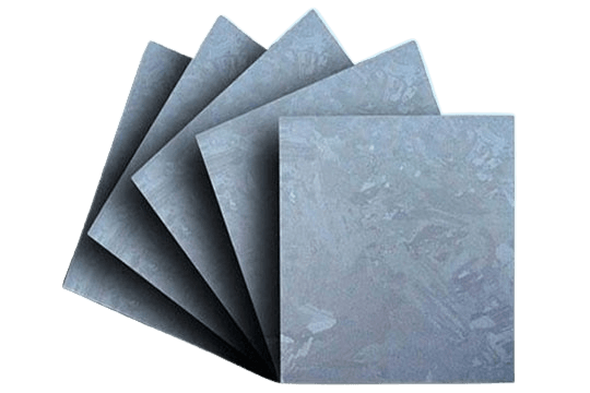
Polysilicon (Multicrystalline) Wafer
Polysilicon (Multicrystalline) wafers are essential materials for the production of photovoltaic cells, playing a crucial role in various industries. These wafers are widely used in photovoltaic power generation, communications, transportation, and residential power supply, especially in remote areas. They also find applications in emerging fields such as solar lighting, lawn solar power, and rooftop solar energy systems.
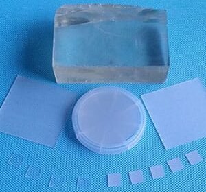
The Polysilicon (Multicrystalline) wafers produced by TFM are known for their superior surface quality and high conversion efficiency, ensuring optimal performance and reliability in a range of applications.
Specifications
| Materials | Polysilicon (Multicrystalline) Wafer | ||
|---|---|---|---|
| Symbol | Si | ||
| Process | Diamond wire cutting | ||
| Conduction type/ Dopant | P-type or N-type | ||
| Side width | 156.75.00~157.25mm | ||
| Thickness | 200±20μm | ||
| Conversion efficiency | >18.8% | ||
Technical Data
| Material Characters | ||
|---|---|---|
| Crystal Growth Method | DSS | – |
| Conduction type/ Dopant | P/Boron, Gallium | Conductivity type tester |
| Resistivity (Ω·cm) | 0.8~3.5 | Non-contact testing |
| Lifetime of brick (μs) | ≥4 μs | Semilab WT-2000D |
| Textured Surface Reflectivity | 17.5% ± 2.5% | Standard Diffusion 8 Integration Spheree Spectroscopic-Reflectometer |
| Oxygen Concentration (atoms/cm3) | ≤5.0E17 (10ppma) | FTIR(ASTM F1188) |
| Carbon Concentration (atoms/cm3) | ≤5.0E17 (10ppma) | FTIR(ASTM F1391) |
Properties
| Dimension | ||
|---|---|---|
| Side Length | 156.75/157.25±0.25 mm | Digital vernier caliper or wafer inspection system |
| Thickness | 170-200 μm | Wafer inspection system |
| TTV | ≤30 μm | Wafer inspection system |
| Saw mark | ≤15 μm | Wafer inspection system |
| Warpage | ≤50 μm | Wafer inspection system |
| Verticality of side | 90 o±0.3o | Wafer inspection system (CCD) |
| Chamfer Hypotenuse | 0.45~ 2.00 mm | VernierCaliper /CCD |
| Chamfer Cathetus | 0.31~ 1.42 mm | |
| Chamfer angle | 45 o±10o | |
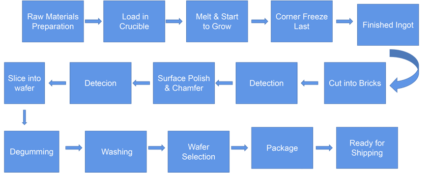
Description
Packing
200 pcs/foam box → 10 foam Boxes/ Carton→ 24 Cantoms/ Wooden Pallet
Reviews
There are no reviews yet.