Generic selectors
Exact matches only
Search in title
Search in content
Post Type Selectors

ST0980 Potassium Sodium Niobate Sputtering Target, KNaNb2O6

Chemical FormulaKNaNbO3
Catalog No.ST0980
CAS Number
Purity99.9%, 99.95%, 99.99%, 99.995%, 99.999%
ShapeDiscs, Plates, Column Targets, Step Targets, Custom-made

With an emphasis on superior quality and cost-effectiveness, TFM offers Potassium-Sodium Niobate sputtering targets. Our competitive pricing makes these targets an excellent choice for a range of high-tech applications, ensuring that clients receive premium quality while maintaining affordability.

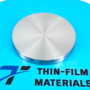
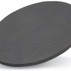
Potassium Sodium Niobate Sputtering Target Description

Potassium-Sodium Niobate sputtering targets are distinguished by their exceptional performance in the semiconductor and electronics sectors, thanks to their superior electrical properties. Their chemical stability during film preparation ensures consistent performance under various environmental conditions, enhancing their versatility.

The unique alloy combination of these targets provides the ability to adjust physical properties, which is crucial for tailoring thin films to meet specific application requirements. This feature is particularly valuable across a range of industries, including semiconductors, electronics, and optics. The adaptable nature of Potassium-Sodium Niobate sputtering targets makes them essential for advancing thin film deposition technologies and supporting innovations in high-tech applications.

Related Product: Potassium Niobate Sputtering Target, Potassium Sputtering Target

Potassium Sodium Niobate Sputtering Target Specifications

Compound FormulaKNaNbO3
AppearanceGrey Target
Available SizesDia.: 1.0″, 2.0″, 3.0″, 4.0″, 5.0″, 6.0″

Thick: 0.125″, 0.250″

Potassium Sodium Niobate Sputtering Target Handling Notes

Indium bonding is recommended for Potassium-Sodium Niobate sputtering targets due to their inherent characteristics, such as brittleness and low thermal conductivity, which can impact sputtering performance. The low thermal conductivity and susceptibility to thermal shock make indium bonding an effective solution to enhance the stability and efficiency of these targets during the sputtering process.

Potassium Sodium Niobate Sputtering Target Application

Semiconductor Manufacturing: In the semiconductor industry, Potassium-Sodium Niobate sputtering targets are utilized for thin film deposition, offering exceptional electrical performance that supports the preparation of electronic components and integrated circuits.

Optical Coatings: Thanks to their excellent physical properties, these targets are crucial in the production of optical coatings. They help create thin films with specialized optical characteristics, such as those used in filters and lenses.

Electronic Device Manufacturing: Potassium-Sodium Niobate sputtering targets are extensively used in the manufacturing of electronic devices. They facilitate the preparation of thin films that enhance the performance and stability of electronic components.

Potassium Sodium Niobate Sputtering Target Packaging

Our Potassium-Sodium Niobate sputtering targets are meticulously handled throughout storage and transportation to ensure they maintain their quality and arrive in pristine condition.

Get Contact

TFM’s Potassium-Sodium Niobate sputtering targets are available in a variety of forms, purities, and sizes. We specialize in manufacturing high-purity physical vapor deposition (PVD) materials with maximum density and minimal average grain sizes, suitable for semiconductor, chemical vapor deposition (CVD), and PVD applications in display and optical technologies. Contact us now to make an inquiry.

Reviews

There are no reviews yet.

Be the first to review “ST0980 Potassium Sodium Niobate Sputtering Target, KNaNb2O6”

Your email address will not be published. Required fields are marked *

Related Products

FAQ

It’s the source material (in solid form) used in sputter deposition to eject atoms or molecules that then form a thin film on a substrate.

Targets can be pure metals (e.g., gold, copper, aluminum), ceramics (e.g., Al₂O₃, SiO₂, TiO₂), alloys, or composites—chosen based on the film’s desired properties.


They are produced by processes such as melting/casting for metals or sintering (often with hot isostatic pressing) for ceramics and composite targets to ensure high density and purity.


In a vacuum chamber, a plasma (typically argon) bombards the target, ejecting atoms that travel and condense on a substrate, forming a thin film.


Key factors include the target’s purity, density, grain structure, and the sputtering yield (i.e. how many atoms are ejected per incident ion), as well as operating conditions like power density and gas pressure.


Operators monitor target erosion (often by measuring the depth of the eroded “race track”) or track total energy delivered (kilowatt-hours) until it reaches a threshold that can compromise film quality.


Fragile materials (such as many ceramics or certain oxides) and precious metals often require a backing plate to improve cooling, mechanical stability, and to allow thinner targets that reduce material costs.


DC sputtering is used for conductive targets, while RF sputtering is necessary for insulating targets (like many oxides) because it prevents charge buildup on the target’s surface.


In reactive sputtering, a reactive gas (e.g., oxygen or nitrogen) is introduced to form compound films on the substrate, but it may also “poison” the target surface if not carefully controlled.


Many manufacturers prefer to control raw material quality by sourcing their own powders; using external powders can risk impurities and inconsistent target properties.


Targets should be stored in clean, dry conditions (often in original packaging or re-wrapped in protective materials) and handled with gloves to avoid contamination, ensuring optimal performance during deposition.

Deposition rate depends on factors such as target material and composition, power density, working gas pressure, substrate distance, and the configuration of the sputtering system (e.g., magnetron design).

 
Shopping Cart
Scroll to Top