
Samarium Nickel Oxide Sputtering Target Description
We proudly introduce Samarium Nickel Oxide Sputtering Targets, distinguished by their remarkable purity and unique material composition. This exceptional purity ensures the targets’ efficacy in precise thin-film deposition processes, playing a vital role in the creation of high-quality electronic devices. The distinctive magnetic and electronic characteristics inherent in Samarium Nickel Oxide make these targets invaluable in applications ranging from electronics to magnetics and sensor technologies. Our commitment to excellence is underscored by the provision of these targets, contributing significantly to advancements in materials engineering and deposition technologies. The exceptional properties of Samarium Nickel Oxide Sputtering Targets position them at the forefront of cutting-edge technological innovations.
Related Product: Samarium Sputtering Target, Samarium Oxide Sputtering Target
Samarium Nickel Oxide Sputtering Target Specifications
| Compound Formula | SmNiO3 |
| Molecular Weight | 257.05 |
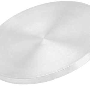
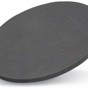
| Appearance | Black Target |
| Density | 7.79 g/cm3 |
| Available Sizes | Dia.: 1.0″, 2.0″, 3.0″, 4.0″, 5.0″, 6.0″ Thick: 0.125″, 0.250″ |
Samarium Nickel Oxide Sputtering Target Handling Notes
Indium bonding is recommended for the Samarium Nickel Oxide Sputtering Target due to its characteristics that are not amenable to sputtering, such as brittleness and low thermal conductivity. This material’s low thermal conductivity and susceptibility to thermal shock make it necessary to use indium bonding to ensure optimal performance during sputtering.
Samarium Nickel Oxide Sputtering Target Application
- Electronics: Samarium Nickel Oxide Sputtering Targets are integral to electronics manufacturing, contributing to the creation of high-performance electronic devices with their unique electronic properties.
- Magnetics: The targets are crucial in magnetics, where their distinctive magnetic characteristics play a pivotal role in developing precise and efficient magnetic components.
- Sensor Technologies: Samarium Nickel Oxide is valuable in sensor technologies, showcasing its versatility and adaptability in creating advanced sensors with enhanced functionalities.
- Thin-Film Deposition: These targets are instrumental in thin-film deposition processes, ensuring precise and uniform coatings essential for various industrial and research applications.
- Materials Engineering Advancements: SAM provides these targets with a commitment to excellence, contributing significantly to advancements in materials engineering and deposition technologies.
Samarium Nickel Oxide Sputtering Target Packaging
Our Samarium Nickel Oxide Sputtering Target is meticulously handled during storage and transportation to maintain the quality of the product in its original condition.

Reviews
There are no reviews yet.