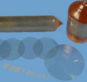
Sapphire Wafer (Al2O3)
Sapphire Wafer (Al2O3) is a highly versatile substrate, widely recognized for its exceptional mechanical strength, high thermal conductivity, and electrical insulation properties. These wafers are integral to various applications, including semiconductor devices, optoelectronic components, and LED technology. With superior purity and a hexagonal crystal structure, Sapphire wafers ensure outstanding performance in high-performance electronic and optical applications.
Physical Properties
- Material: Al2O3 (Aluminum Oxide)
- Crystal Structure: Hexagonal
- Lattice Constants: a = 4.758 Å, c = 12.992 Å
- Crystal Purity: >99.99%
- Density: 3.98 g/cm³
- Melting Point: 2040°C
- Hardness: 9.0 on the Mohs scale
- Thermal Expansion: 7.5 × 10⁻⁶/°C
- Thermal Conductivity: 46.06 W/(m·K) at 0°C, 25.12 W/(m·K) at 100°C, 12.56 W/(m·K) at 400°C
- Dielectric Constants: 9.4 at 300K (A axis), 11.58 at 300K (C axis)
- Loss Tangent at 10 GHz: < 2 × 10⁻⁵ at A axis, < 5 × 10⁻⁵ at C axis
Specifications
- Size Options: 10×3, 10×5, 10×10, 15×15, 20×15, 20×20, Dia 15, Dia 20, Dia 1”
- Thickness: 0.5 mm, 1.0 mm
- Polished: SSP or DSP
- Crystallographic D Spacing:
- (1120) – a plane: 2.379 Å
- (1102) – r plane: 1.740 Å
- (1010) – m plane: 1.375 Å
- (1123) – n plane: 1.147 Å
- (0001) – c plane: 2.165 Å
- (1011) – s plane: 1.961 Å
- Redirection Precision: ±0.5°
- Redirection the Edge: 2° (special in 1° available)
- Angle of Crystalline: Custom sizes and orientations available upon request
- Surface Roughness (Ra): ≤5Å (5µm × 5µm)
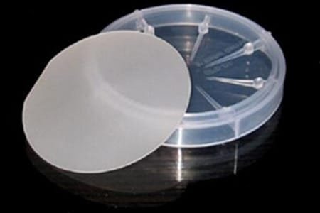
Packaging
Sapphire Wafers are packaged in class 100 clean bags or wafer containers within a class 1000 clean room environment to ensure pristine conditions during handling and transport.
Ideal for high-tech industries such as optoelectronics, semiconductors, and LED production, Sapphire Wafer (Al2O3) substrates provide a reliable solution for demanding applications.
Reviews
There are no reviews yet.