Generic selectors
Exact matches only
Search in title
Search in content
Post Type Selectors

ScAlMgO4 Substrate

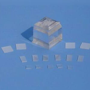
TFM’s ScAlMgO₄ Substrate

TFM offers high-quality ScAlMgO4 (Scandium Aluminum Magnesium Oxide) substrates, known for their excellent lattice matching, thermal stability, and superior surface quality. These substrates are widely used in advanced thin-film applications, particularly for epitaxial growth of high-performance electronic and optoelectronic materials.

ScAlMgO₄ substrates feature a low lattice mismatch with III-nitride materials, making them ideal for GaN-based device fabrication, including LEDs, high-frequency transistors, and power electronics. Their high thermal conductivity ensures efficient heat dissipation, enhancing device performance and longevity. Additionally, the low defect density and atomically smooth surface contribute to high-quality film growth, improving overall device efficiency.

TFM provides precisely engineered ScAlMgO₄ substrates to meet the demanding requirements of modern semiconductor research and production, ensuring optimal performance for next-generation electronic and photonic applications.

ScAlMgO₄ Substrate Specifications

SpecificationDetails
MaterialScAlMgO₄
Lattice (Å)a = 0.3246, c = 2.5195
StructureM6
Orientation<0001>
Size20 x 20 mm, 10 x 10 mm, 10 x 5 mm, 5 x 5 mm
Thickness400 μm, 500 μm ± 25 μm

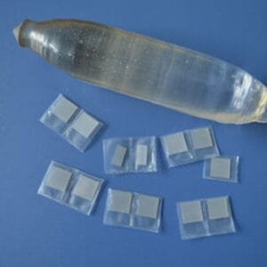
ScAlMgO₄ Substrate Packaging

TFM ensures safe and contamination-free delivery by packaging ScAlMgO₄ substrates in a class 100 clean bag or wafer container within a class 1000 clean room.

Choose TFM for premium ScAlMgO₄ substrates designed to meet the highest industry standards for semiconductor growth and research applications.

Reviews

There are no reviews yet.

Be the first to review “ScAlMgO4 Substrate”

Your email address will not be published. Required fields are marked *

FAQ

A thin film substrate is the base material upon which thin layers of materials are deposited to create electronic, optical, or mechanical devices. The substrate provides structural support and can influence the properties of the thin film.

The choice of substrate affects the film’s structural integrity, electrical properties, and overall performance. Factors like thermal expansion coefficient, surface smoothness, and chemical compatibility are crucial considerations.

Materials such as lanthanum aluminate (LaAlO₃), magnesium oxide (MgO), and strontium titanate (SrTiO₃) are commonly used due to their lattice compatibility and thermal stability, which are essential for optimal superconducting properties.

Metal substrates offer high electrical and thermal conductivity, making them suitable for applications requiring efficient heat dissipation and electrical connectivity. However, their surface properties and potential for oxidation must be managed during deposition.

These substrates are materials that can support the growth of thin films exhibiting magnetic or ferroelectric properties, essential for applications in memory devices, sensors, and actuators.

Semiconductor substrates, such as silicon wafers, serve as the foundation for integrated circuits and various electronic components, providing the necessary electrical characteristics and structural support for device fabrication.

Gallium Nitride (GaN) substrates are pivotal for high-performance optoelectronic and power devices due to their excellent thermal conductivity, high breakdown voltage, and efficiency. They are widely used in LEDs, power transistors, and RF components.

Halide crystal substrates, composed of halide compounds, are utilized in specialized optical applications, including infrared spectroscopy and laser systems, due to their unique optical properties.
Ceramic substrates provide high thermal stability, mechanical strength, and electrical insulation, making them ideal for high-frequency and high-power applications.
Proper surface preparation, including cleaning and polishing, ensures the removal of contaminants and surface irregularities, leading to improved film adhesion, uniformity, and performance.
Yes, thin films can be deposited on flexible substrates like polymers, enabling the development of flexible electronics and wearable devices. However, challenges include managing mechanical stress and ensuring film adhesion.
Challenges include ensuring lattice matching to minimize defects, managing thermal expansion differences to prevent stress and delamination, and achieving desired electrical and optical properties for specific applications.
Shopping Cart
Scroll to Top