
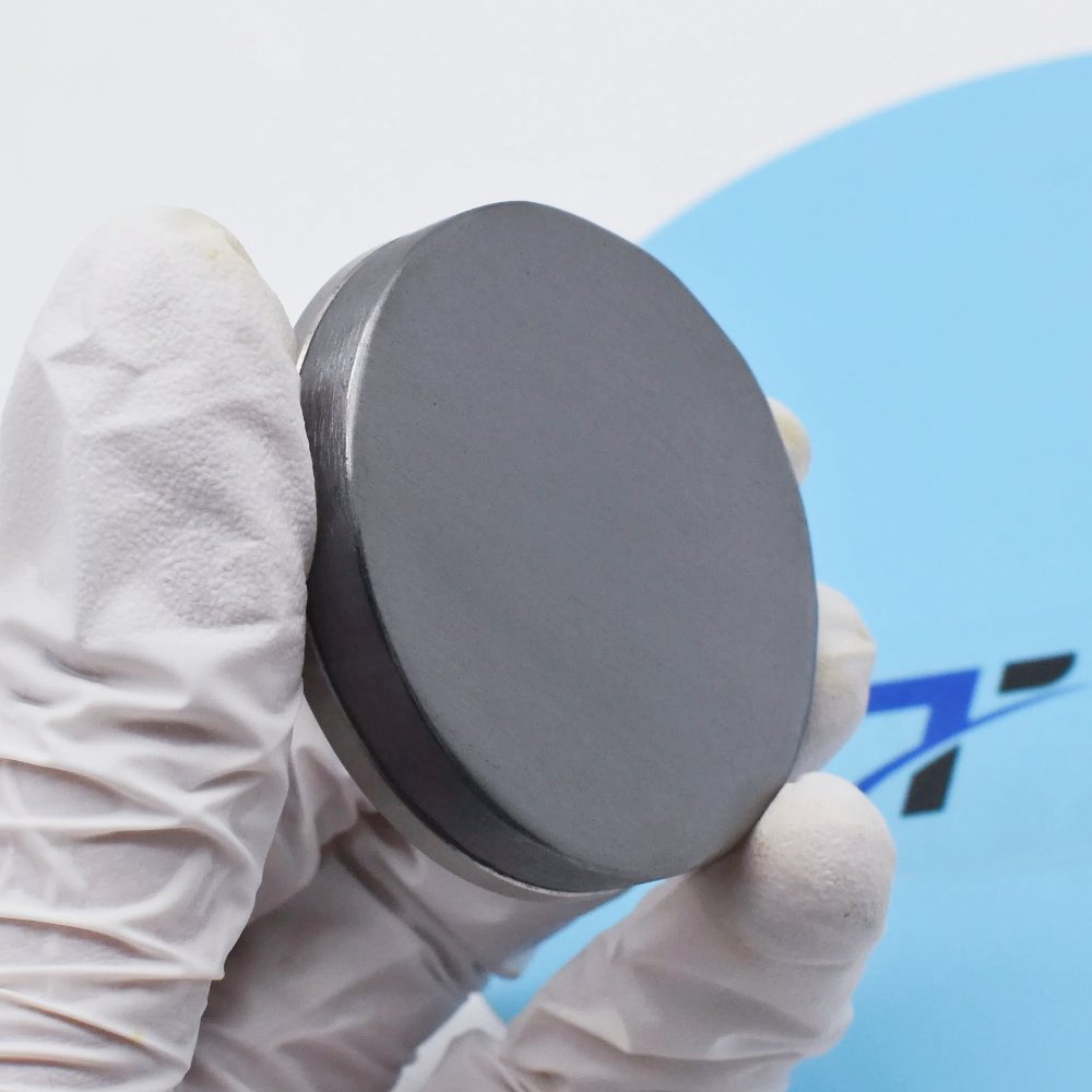

What is a selenium sputtering target?
A selenium sputtering target is an elemental Se source used to deposit selenium-containing films by sputtering, either as a direct layer or as one source in compound and co-sputtered film development. The RFQ should define the purity basis, target geometry, cathode and backing requirements, intended power mode, and film acceptance measurements. Target composition identifies the source material, but the deposited film must be verified under the intended process.
Use the Sputtering Targets catalog when the source material or target format is still being selected.


Material and Deposition Characteristics
The preferred power mode depends on the target’s electrical resistivity and the deposition system. Some elemental targets in this family can be processed with DC or pulsed-DC sputtering, while others may require RF sputtering or more conservative operating conditions. When the deposited film acts as a precursor layer for a compound or multilayer system, film analysis is recommended to verify the final composition and structure.
Selenium sputtering target selection data
| Selection field | What to specify | Why it matters |
|---|---|---|
| Material identity | Elemental selenium (Se) and the required purity basis | Defines the source material and the contamination limits to review |
| Target geometry | Shape, finished dimensions, tolerances, quantity, and drawing revision | Connects the material requirement to the actual cathode interface |
| Power and process context | Intended RF, DC, pulsed-DC, or other mode plus operating constraints | Power compatibility must be confirmed for the target and equipment combination |
| Backing and bonding | Cathode model, backing material and dimensions, interface request, cooling, and operating context | Allows mechanical support and thermal-path requirements to be reviewed together |
| Film acceptance | Required composition, contamination, thickness, optical, electrical, structural, or phase measurements | Compound or composition-sensitive films require process-specific verification |
| Inspection and documents | List dimensional, composition, visual, packaging, or lot-document evidence required | Keeps order acceptance criteria separate from generic catalog statements |
Typical Thin-Film Applications
- Elemental selenium films and precursor-layer development
- Chalcogenide, optical, electronic, infrared, thermoelectric, or phase-change studies where the approved design specifies selenium
- Co-sputtering or subsequent compound-formation projects with defined composition and phase measurements
Application fit depends on the complete layer design and qualified deposition process. Review the broader thin-film application categories before finalizing the target RFQ.
Target Configuration and Ordering Considerations
For a selenium target quotation, provide the purity basis, target shape and finished dimensions, drawing revision, quantity, cathode model, backing and interface requirements, intended power mode, cooling and operating context, plus any tolerance, packaging, inspection, or lot-document requirements. Send the available drawing and acceptance criteria to TFM for review; unlisted dimensions, bonding, purity, packaging, and documentation requirements remain subject to quotation and approved specification.
Frequently Asked Questions
What is a Selenium sputtering target typically used for?
It is used either to deposit the elemental film directly or to serve as a source component in compound, optical, electronic, chalcogenide, or other functional thin-film systems.
Should Selenium be sputtered with DC or RF power?
The best power mode depends on target resistivity, dimensions, and sputtering-system capability. Some elemental targets in this family can work with DC or pulsed-DC power, while others are more commonly evaluated with RF power.
Why is purity important for a Selenium target?
Many of these materials are used in composition-sensitive thin films, so metallic or chemical impurities can affect the behavior of the final film or multilayer stack. The target purity should therefore be matched to the application.
Can a Selenium target be ordered as a bonded assembly?
A bonded assembly request should include the cathode model or drawing, target dimensions, backing material and dimensions, interface requirement, cooling, and operating context. Availability and the final assembly specification must be confirmed in the quotation.
Does target composition guarantee film composition for Selenium?
Not always. Film composition can shift because of sputtering conditions, substrate temperature, chamber history, and re-sputtering effects. Film analysis is recommended when the final composition is critical.
What should be included in an RFQ for Selenium?
Provide purity, dimensions, quantity, target configuration, backing requirement if any, cathode model or drawing, and any special packaging or inspection-document requirements.
Prepare your RFQ: Download the fillable Selenium Sputtering Target, Se RFQ Worksheet (PDF). Enter the required composition or grade, dimensions, backing or bonding request, quantity, documents, and acceptance criteria for quotation review.



Reviews
There are no reviews yet.