 MSDS File
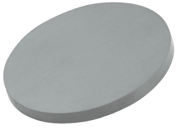
Silicon Carbide Sputtering Target Description
Silicon Carbide sputtering target from TFM is a carbide ceramic material with the chemical formula SiC.
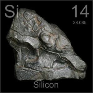 Silicon is a chemical element that originated from the Latin words ‘silex’ or ‘silicis,’ meaning flint. It was first mentioned in 1824 and observed by J. Berzelius, who also accomplished its isolation and announced it. The canonical chemical symbol for silicon is “Si,” and it has an atomic number of 14. Silicon is located in Period 3 and Group 14 of the periodic table, belonging to the p-block. Its relative atomic mass is 28.0855(3) Dalton, with the number in brackets indicating the measurement uncertainty.
Related Product: P-Type Silicon Sputtering Target
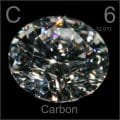 Carbon is a chemical element that traces its name to the Latin word ‘carbo,’ meaning charcoal. It has been in use since at least 3750 BC, first discovered by ancient civilizations such as the Egyptians and Sumerians. The chemical symbol for carbon is “C,” and it has an atomic number of 6. Positioned in Period 2 and Group 14 of the periodic table, carbon is part of the p-block elements. Its relative atomic mass is 12.0107(8) Dalton, with the number in parentheses indicating the uncertainty of the measurement.
Silicon Carbide Sputtering Target Specification
| Material Type | Silicon Carbide |
| Symbol | SiC |
| Melting Point (°C) | ~2,700 |
| Theoretical Density (g/cc) | 3.22 |
| Sputter | RF |
| Type of Bond | Indium, Elastomer |
| Comments | Sputtering preferred. |
Silicon Carbide Sputtering Target Bonding Services
Specialized bonding services for Silicon Carbide Sputtering Targets, including indium and elastomeric bonding techniques, enhance performance and durability. Thin Film Materials (TFM) ensures high-quality solutions that meet industry standards and customer needs.
We also offer custom machining of backing plates, which is essential for sputtering target assembly. This comprehensive approach improves target design flexibility and performance in thin film deposition. Our channels provide detailed information about bonding materials, methods, and services, helping clients make informed decisions.

Silicon Carbide Sputtering Target Packaging
Our Silicon Carbide Sputtering Target is meticulously tagged and labeled externally to guarantee accurate identification and maintain strict quality control. We exercise great caution during handling and packaging to prevent any potential damage during storage or transportation, ensuring the product reaches you in pristine condition.

Reviews
There are no reviews yet.