Introduction
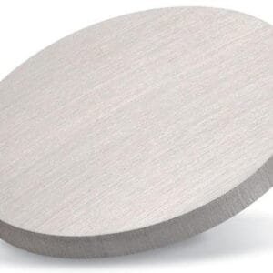
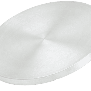
Silicon (Si) Rotary Sputtering Target
TFM offers high-quality Silicon (Si) rotary sputtering targets, ideal for thin-film deposition in various semiconductor and photovoltaic applications. Silicon targets are essential for producing high-purity silicon films, which are widely used in semiconductor device fabrication, solar cells, and microelectromechanical systems (MEMS).
The rotary sputtering target design ensures uniform and efficient deposition of silicon films with excellent adhesion and thin-film properties, critical for applications such as integrated circuits (ICs), photoelectric devices, and sensors. The high-density and low impurity levels of the Si targets ensure superior quality films for next-generation electronics and optical coatings.
TFM supplies customized Silicon (Si) rotary sputtering targets, offering precise control over composition, purity, and deposition parameters. These targets are engineered for optimal performance, meeting the stringent requirements of industries like semiconductors, solar energy, and electronics.
Specifications
| Materials | Silicon (Si) Rotary Sputtering Target |
|---|---|
| Symbol | Si |
| Conduction Type | P-type doped Boron, N-type doped Phosphorus |
| Purity | 99.9% – 99.999% |
| Theoretical Density (g/cc) | 2.32 |
| Melting Point (°C) | 1,410 |
| Production Method | Spraying Type, Bonded Type (CZ) |
| Backing Tube | Titanium, Stainless Steel |
| Resistivity (Ω.cm) | 0.01 – 400 |
| Size | As per customer’s drawings |
| Relative Density | >= 96% |
| Grain Sizes | < 100 µm |
| Annual Capacity | 1000 tons |
Applications
- SiO2/Si3N4 Film
- Thin Film Photovoltaic Solar Industry
- Semiconductor Electronics Industry
- Flat Panel Display Industry
- Construction / Automotive Glass Industry
- Optical Industry
- Decorative / Functional Coating Industry

 MSDS File


Reviews
There are no reviews yet.