Introduction
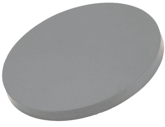
The Strontium Niobium Titanate Sputtering Target is a complex oxide ceramic target widely used for depositing functional thin films with advanced electrical and dielectric properties. As a member of the perovskite oxide family, strontium niobium titanate exhibits excellent electrical conductivity, dielectric stability, and tunable electronic behavior, making it valuable for oxide electronics, thin film capacitors, sensors, and advanced semiconductor research.
Through magnetron sputtering or other physical vapor deposition (PVD) techniques, strontium niobium titanate targets allow the formation of high-quality oxide thin films with controlled composition and microstructure. These materials are particularly important in the development of functional oxide devices and emerging electronic materials.
Detailed Description
Strontium Niobium Titanate sputtering targets are typically manufactured from high-purity precursor oxides including strontium oxide (or carbonate), niobium oxide, and titanium oxide. These powders are carefully mixed, calcined, and sintered through advanced ceramic processing techniques such as hot pressing, vacuum sintering, or hot isostatic pressing (HIP) to achieve high density and homogeneous composition.
The resulting material typically adopts a perovskite-type crystal structure, which is well known for its versatile electronic and dielectric properties. By adjusting the relative proportions of niobium and titanium within the lattice, researchers can tailor the electrical conductivity, dielectric constant, and carrier concentration of the material.
Niobium acts as a donor dopant that can increase electrical conductivity, while titanium contributes to the structural stability and dielectric behavior of the compound. This combination enables thin films with tunable electronic properties, making them suitable for a variety of electronic and electrochemical applications.
High-density sputtering targets ensure stable plasma conditions during deposition and minimize particle generation, which is essential for producing uniform thin films. For high-power sputtering systems, strontium niobium titanate targets can also be supplied as bonded targets with copper backing plates, typically using indium bonding to improve heat dissipation and mechanical stability.
Applications
Strontium Niobium Titanate sputtering targets are used in a range of advanced technology areas:
Oxide electronic devices requiring functional perovskite thin films
Thin film capacitors and dielectric layers in microelectronics
Sensors and electrochemical devices utilizing conductive oxide films
Transparent conductive oxide research in advanced materials development
Ferroelectric and dielectric thin film studies
Academic and industrial research laboratories studying perovskite oxides
Technical Parameters
| Parameter | Typical Value / Range | Importance |
|---|---|---|
| Chemical Composition | Sr–Nb–Ti–O complex oxide | Determines electrical and dielectric behavior |
| Purity | ≥ 99.9% | Ensures stable thin film properties |
| Diameter | 25 – 300 mm (custom) | Compatible with common sputtering systems |
| Thickness | 3 – 6 mm | Influences sputtering stability and target lifetime |
| Density | ≥ 95% theoretical density | Supports uniform film deposition |
| Bonding | Copper backing plate / Indium bonded | Improves heat transfer and target durability |
Comparison with Related Materials
| Material | Key Advantage | Typical Application |
|---|---|---|
| Strontium Niobium Titanate | Tunable conductivity and dielectric properties | Functional oxide electronics |
| Strontium Titanate (SrTiO₃) | High dielectric constant and good lattice compatibility | Substrates and dielectric films |
| Niobium Oxide (Nb₂O₅) | High dielectric constant | Capacitors and optical coatings |
FAQ
| Question | Answer |
|---|---|
| What sputtering methods are suitable for this target? | Strontium Niobium Titanate sputtering targets are typically used in RF magnetron sputtering systems suitable for ceramic materials. |
| Can the target composition be customized? | Yes. The ratio of strontium, niobium, and titanium can be adjusted depending on the desired electronic properties. |
| Are bonded sputtering targets available? | Yes. Targets can be bonded to copper backing plates to improve heat dissipation during sputtering. |
| What substrates can these films be deposited on? | Films can be deposited on silicon wafers, glass, ceramic substrates, and other oxide materials. |
| What purity levels are typically available? | Standard purities typically range from 99.9% and above for advanced electronic applications. |
Packaging
Our Strontium Niobium Titanate Sputtering Target products are meticulously tagged and labeled externally to ensure efficient identification and maintain high standards of quality control. Each target is carefully packaged in vacuum-sealed bags with protective foam and export-grade cartons or wooden crates to prevent contamination and mechanical damage during storage and transportation.
Conclusion
The Strontium Niobium Titanate Sputtering Target provides a reliable solution for depositing functional oxide thin films used in advanced electronic and electrochemical devices. Its perovskite structure and tunable electrical properties make it an important material for oxide electronics, dielectric devices, and materials research.
With customizable compositions, high-density ceramic manufacturing, and stable sputtering performance, strontium niobium titanate sputtering targets support both industrial thin film production and cutting-edge research in functional oxide materials.
For detailed specifications and a quotation, please contact us at sales@thinfilmmaterials.com.


Reviews
There are no reviews yet.