 MSDS File
Introduction
Tantalum Diselenide Evaporation Materials (TaSe₂) are advanced transition metal dichalcogenide (TMD) sources designed for precision thin film deposition in electronics, optoelectronics, and two-dimensional (2D) materials research. As a layered compound with unique charge density wave (CDW) behavior and metallic conductivity, TaSe₂ plays an important role in next-generation device architectures and fundamental condensed matter studies.
In vacuum evaporation processes, maintaining compound stoichiometry and minimizing selenium loss are essential. Carefully synthesized TaSe₂ evaporation materials provide consistent composition, controlled phase structure, and reliable performance for both laboratory-scale research and pilot production systems.
Detailed Description
Tantalum Diselenide (TaSe₂) is a layered TMD compound in which tantalum atoms are sandwiched between selenium layers, forming van der Waals-bonded structures. This intrinsic layered nature makes TaSe₂ particularly attractive for 2D material fabrication and exfoliation-based applications.
Key characteristics include:
Stoichiometric TaSe₂ Composition – Controlled Ta:Se ratio ensures predictable electrical and structural properties.
High Purity Grades (3N–5N typical) – Reduces oxygen and metallic impurities that may disrupt electronic performance.
Phase-Controlled Material – Typically supplied in the stable 2H phase; other phases may be available upon request.
Optimized Particle Size or Crystalline Form – Supports uniform evaporation and reduces spitting in vacuum systems.
Due to selenium’s relatively higher vapor pressure compared to tantalum, deposition parameters must be optimized to maintain film stoichiometry. Electron beam evaporation is commonly used, with gradual power ramping to prevent compound decomposition or selenium deficiency.
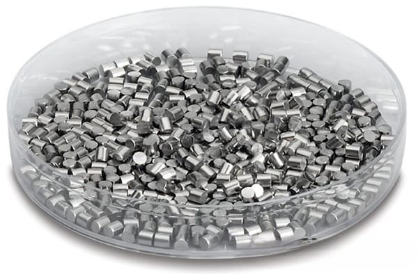
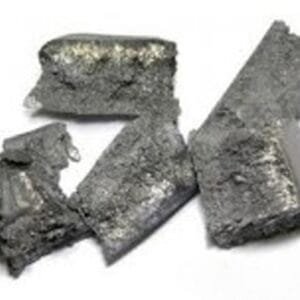
TaSe₂ evaporation materials are supplied as powder, granules, or crystalline pieces, compatible with graphite crucibles, molybdenum liners, or e-beam hearth systems.
Applications
Tantalum Diselenide Evaporation Materials are widely used in:
2D Materials Research
Fabrication of layered TaSe₂ films for electronic and quantum material studies.Charge Density Wave (CDW) Investigations
Thin films for studying phase transitions and electronic instabilities.Nanoelectronics & Spintronics
Metallic TMD layers in advanced device structures.Heterostructure Engineering
Integration with other TMDs (e.g., MoS₂, WS₂) for layered material stacks.Advanced Thin Film R&D
Exploration of transition metal chalcogenide properties in vacuum-deposited films.
Technical Parameters
| Parameter | Typical Value / Range | Importance |
|---|---|---|
| Purity | 99.9% – 99.999% (3N–5N) | Minimizes defect formation in films |
| Chemical Formula | TaSe₂ | Ensures proper compound stoichiometry |
| Phase | 2H (standard) | Defines electronic structure |
| Form | Powder / Granules / Crystals | Compatible with evaporation systems |
| Melting Behavior | Compound-dependent (~ >1200°C) | Influences evaporation strategy |
| Packaging | Vacuum-sealed / inert atmosphere | Prevents oxidation and Se loss |
Comparison with Related TMD Materials
| Material | Key Advantage | Typical Application |
|---|---|---|
| Tantalum Diselenide (TaSe₂) | Metallic conductivity & CDW behavior | Quantum & electronic films |
| Molybdenum Disulfide (MoS₂) | Semiconducting 2D material | Transistors & sensors |
| Tungsten Diselenide (WSe₂) | Direct bandgap in monolayer form | Optoelectronics |
| Niobium Diselenide (NbSe₂) | Superconducting properties | Low-temperature physics |
Compared to semiconducting TMDs, TaSe₂ exhibits metallic conductivity and charge density wave phenomena, making it particularly suitable for fundamental physics research and advanced electronic applications.
FAQ
| Question | Answer |
|---|---|
| Is TaSe₂ suitable for thermal evaporation? | It can be used, but electron beam evaporation is generally preferred for better stoichiometric control. |
| How is stoichiometry maintained during deposition? | Process optimization, controlled heating, and stable vacuum conditions are essential to minimize selenium loss. |
| Can purity levels be customized? | Yes, various purity grades are available based on research or production requirements. |
| What form is supplied? | Powder, granules, and crystalline pieces can be provided to match system compatibility. |
| Which industries use TaSe₂ films most? | Research institutions, nanoelectronics labs, quantum materials research, and advanced semiconductor development. |
Packaging
Our Tantalum Diselenide Evaporation Materials are meticulously tagged and labeled externally to ensure efficient identification and maintain high standards of quality control. We take great care to prevent any potential damage during storage and transportation, ensuring the materials arrive in perfect condition.
Conclusion
Tantalum Diselenide Evaporation Materials (TaSe₂) offer a reliable and high-purity source for the deposition of layered transition metal dichalcogenide thin films. With controlled composition, phase integrity, and flexible supply formats, TaSe₂ supports cutting-edge research and next-generation electronic material development.
For detailed specifications and a quotation, please contact us at sales@thinfilmmaterials.com.

Reviews
There are no reviews yet.