 MSDS File
Introduction
Tantalum Silicide (TaSi₂) evaporation materials are widely used in advanced thin film deposition processes where high thermal stability, excellent electrical conductivity, and strong chemical resistance are required. As a refractory silicide compound, TaSi₂ plays a critical role in semiconductor fabrication, diffusion barrier layers, and high-temperature coatings, particularly in vacuum evaporation systems such as electron beam (e-beam) and thermal evaporation.
Detailed Description
Tantalum Silicide (TaSi₂) is an intermetallic compound combining the refractory properties of tantalum with the semiconducting characteristics of silicon. This unique composition provides a balanced combination of high melting point (~2200°C), low electrical resistivity, and excellent oxidation resistance at elevated temperatures.
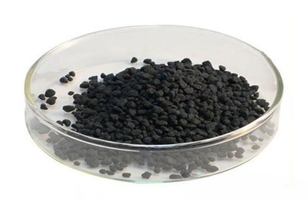
In evaporation applications, TaSi₂ is typically supplied in forms such as granules, pellets, or custom-shaped pieces to ensure uniform evaporation and stable deposition rates. The material’s high density and controlled microstructure help minimize spitting and ensure consistent thin film quality during high-vacuum deposition.
Compared with pure tantalum, TaSi₂ offers improved diffusion barrier performance and reduced stress in deposited films, making it particularly suitable for multilayer structures in microelectronics. Its compatibility with silicon-based substrates further enhances adhesion and film uniformity.
Key features include:
Stable evaporation behavior under high ताप and vacuum conditions
Reduced contamination risk due to controlled purity levels (typically 99.9%–99.99%)
Optimized stoichiometry for consistent film composition
Available in customized sizes to match different evaporation sources (boats, crucibles, liners)
Applications
Tantalum Silicide evaporation materials are used across a wide range of high-tech industries:
Semiconductor device fabrication (diffusion barriers, gate materials)
Thin film resistors and integrated circuits
Optical coatings requiring high-temperature stability
Protective coatings in aerospace and high-temperature environments
Research and development in advanced materials science
Microelectronics and MEMS devices
Technical Parameters
| Parameter | Typical Value / Range | Importance |
|---|---|---|
| Purity | 99.9% – 99.99% | Reduces contamination in thin films |
| Form | Pellets / Granules / Pieces | Ensures controlled evaporation |
| Particle Size | 1 – 6 mm (customizable) | Affects evaporation uniformity |
| Melting Point | ~2200°C | Suitable for high-temperature processes |
| Density | ~9.14 g/cm³ | Influences deposition rate stability |
| Stoichiometry | Ta:Si = 1:2 | Ensures consistent film composition |
Comparison with Related Materials
| Material | Key Advantage | Typical Application |
|---|---|---|
| Tantalum Silicide (TaSi₂) | Excellent thermal stability & conductivity | Semiconductor thin films |
| Tantalum (Ta) | High ductility, pure metal behavior | Adhesion layers, barriers |
| Silicon (Si) | Semiconductor properties | Electronics, photovoltaics |
| Molybdenum Silicide (MoSi₂) | Superior oxidation resistance | High-temperature coatings |
FAQ
| Question | Answer |
|---|---|
| Can TaSi₂ evaporation materials be customized? | Yes, size, shape, and particle range can be tailored for specific evaporation systems. |
| What evaporation methods are suitable? | Commonly used in e-beam evaporation and thermal evaporation under high vacuum. |
| Is the composition strictly controlled? | Yes, precise stoichiometry ensures consistent thin film performance. |
| How should the material be stored? | In dry, vacuum-sealed packaging to prevent oxidation or contamination. |
| What industries use TaSi₂ most? | Semiconductor, electronics, aerospace, and advanced coating industries. |
Packaging
Our Tantalum Silicide Evaporation Materials are meticulously tagged and labeled externally to ensure efficient identification and maintain high standards of quality control. We take great care to prevent any potential damage during storage and transportation, ensuring the materials arrive in perfect condition.
Conclusion
Tantalum Silicide (TaSi₂) evaporation materials offer a reliable solution for high-performance thin film deposition, combining thermal stability, electrical conductivity, and excellent compatibility with semiconductor processes. With flexible customization options and strict quality control, these materials are well suited for both industrial production and advanced research applications.
For detailed specifications and a quotation, please contact us at sales@thinfilmmaterials.com.


Reviews
There are no reviews yet.