 MSDS File
Introduction
Tellurium Evaporation Materials play a critical role in thin film deposition for optoelectronics, photovoltaics, infrared optics, and advanced semiconductor research. As a key chalcogen element, tellurium is widely used to tailor electrical, optical, and thermoelectric properties in functional coatings and compound semiconductor films. High-purity tellurium evaporation materials ensure stable evaporation behavior, precise composition control, and high-quality thin film performance.
Detailed Description
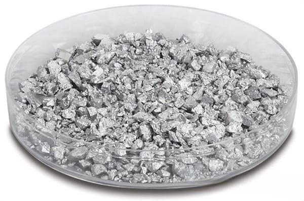
Tellurium evaporation materials are supplied in carefully controlled physical forms—such as pellets, granules, shots, or pieces—optimized for thermal evaporation, electron-beam (e-beam) evaporation, and related PVD processes. High material purity is essential, as trace impurities can significantly affect film conductivity, carrier concentration, and optical absorption.
Our tellurium evaporation materials are refined and processed to achieve uniform composition, low oxygen and metallic impurity levels, and predictable evaporation rates. The material’s relatively low melting point enables efficient evaporation at moderate power levels, while controlled morphology helps minimize spitting and compositional drift during deposition.
Available options include customized purity grades, particle sizes, and packaging formats to suit different evaporation sources, such as boats, crucibles, and liners. Each batch can be supplied with full documentation to support R&D and production requirements.
Applications
Compound semiconductor thin films (e.g., CdTe, HgCdTe, Bi₂Te₃)
Infrared detectors and thermal imaging coatings
Photovoltaic absorber layers and buffer layers
Thermoelectric devices and functional films
Optical coatings and research-scale material studies
Technical Parameters
| Parameter | Typical Value / Range | Importance |
|---|---|---|
| Material | Tellurium (Te) | Core functional element for chalcogenide films |
| Purity | 99.9% – 99.999% | Impurity control affects electrical & optical properties |
| Form | Pellets, granules, shots, pieces | Compatible with different evaporation sources |
| Melting Point | ~449.5 °C | Enables efficient thermal evaporation |
| Deposition Method | Thermal / E-beam evaporation | Flexible PVD compatibility |
| Packaging | Vacuum-sealed, inert protected | Prevents oxidation and contamination |
Comparison with Related Materials (Optional)
| Material | Key Advantage | Typical Application |
|---|---|---|
| Tellurium Evaporation Materials | Precise chalcogen control | Semiconductor & IR films |
| Selenium | Lower evaporation temperature | Photovoltaic buffer layers |
| Sulfur | High vapor pressure | Chalcogenide research films |
FAQ
| Question | Answer |
|---|---|
| Can purity and particle size be customized? | Yes, purity grade and physical form can be tailored to your process. |
| Is tellurium suitable for thermal evaporation? | Yes, its melting point allows stable thermal and e-beam evaporation. |
| How is oxidation prevented during shipping? | Materials are vacuum-sealed or packed under inert atmosphere. |
| Which industries use tellurium most? | Semiconductor, photovoltaics, IR optics, thermoelectrics, and R&D. |
| Is documentation provided? | Certificate of Analysis is available upon request. |
Packaging
Our Tellurium Evaporation Materials are meticulously tagged and labeled externally to ensure efficient identification and strict quality control. Each batch is vacuum-sealed or inert-gas packed with protective cushioning, ensuring the materials arrive in optimal condition without oxidation or physical damage.
Conclusion
Tellurium Evaporation Materials provide reliable composition control, stable evaporation behavior, and high purity for demanding thin film deposition processes. With flexible forms, customizable specifications, and consistent quality, they are well suited for both research-scale experiments and industrial coating applications.
For detailed specifications and a quotation, please contact us at sales@thinfilmmaterials.com


Reviews
There are no reviews yet.