
Tellurium Sputtering Target
Introduction
The Tellurium Sputtering Target from Thin Film Materials (TFM) is a high-purity deposition material widely used in semiconductor, photovoltaic, and optoelectronic applications. Tellurium (Te), a brittle metalloid with semiconductor properties, is highly valued for its role in thin film fabrication due to its unique electrical and optical characteristics. When processed into sputtering targets, Tellurium enables the production of uniform thin films essential for advanced electronics and energy technologies.
Detailed Description
Tellurium sputtering targets are manufactured to ensure high density and excellent purity, typically in the range of 99.9% to 99.999%. This minimizes contamination and guarantees film quality during deposition.
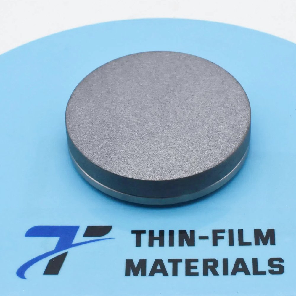
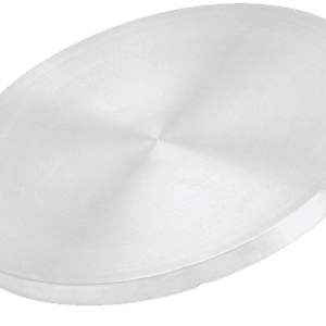
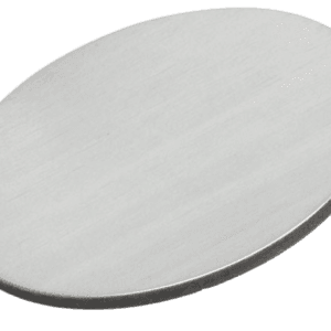
Appearance: Silvery-gray, brittle crystalline solid
Density: ~6.24 g/cm³
Melting Point: 449.5 °C
Crystal Structure: Hexagonal
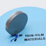
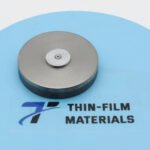
TFM provides Tellurium sputtering targets in standard disc, rectangular, and step target formats. We also offer bonding services with copper or titanium backing plates to enhance durability, improve thermal conductivity, and extend the target’s operational life. Custom machining is available to meet specific sputtering system requirements.
Applications
Tellurium sputtering targets are widely used for:
Semiconductors: compound semiconductors such as CdTe and HgCdTe for detectors and infrared devices
Photovoltaics: thin film solar cells, including CdTe-based solar modules
Optoelectronics: infrared optics, thermoelectric devices, and laser technologies
Research & Development: advanced studies in materials science, energy conversion, and nanotechnology
Technical Parameters
| Parameter | Typical Value / Range | Importance |
|---|---|---|
| Purity | 99.9% – 99.999% | Ensures high-performance films with minimal impurities |
| Diameter | 25 – 150 mm (custom up to 300 mm) | Fits standard and custom sputtering systems |
| Thickness | 3 – 6 mm | Determines sputtering rate and uniformity |
| Bonding Options | Indium / Elastomer | Improves adhesion, heat dissipation, and durability |
| Backing Plate | Copper / Titanium | Supports stability during deposition |
Comparison with Related Materials
| Material | Key Advantage | Typical Application |
|---|---|---|
| Tellurium (Te) | Semiconductor & IR sensitivity | CdTe solar cells, IR optics |
| Cadmium Telluride (CdTe) | High efficiency in photovoltaics | Thin film solar modules |
| Selenium (Se) | Cost-effective chalcogen element | Optoelectronics, glass coatings |
FAQ
| Question | Answer |
|---|---|
| Can Tellurium sputtering targets be customized? | Yes, TFM provides custom sizes, thicknesses, and bonding services. |
| Do you offer bonded targets? | Yes, targets can be bonded with indium or elastomer for enhanced performance. |
| What is the packaging method? | Vacuum-sealed, protected with foam, and shipped in export-safe cartons or crates. |
| Which industries use Tellurium targets most? | Photovoltaics, infrared optics, semiconductors, thermoelectrics, and R&D. |
Packaging
Each Tellurium sputtering target is vacuum-sealed and securely packaged to protect against oxidation and mechanical damage. We ensure safe transport and long-term storage without compromising purity or performance.
Conclusion
The Tellurium (Te) Sputtering Target from TFM offers high purity, superior density, and reliable performance for thin film deposition. With customizable dimensions, bonding services, and consistent quality, our Tellurium targets are ideal for research laboratories and industrial production.
For detailed specifications, quotations, or custom solutions, please contact us at sales@thinfilmmaterials.com.

Reviews
There are no reviews yet.