 MSDS File
Introduction
Tin(II) Fluoride (SnF₂) evaporation materials are specialized compounds used in thin film deposition processes where fluorine-containing coatings are required. With its unique chemical composition, SnF₂ enables the formation of functional fluoride-based films that offer desirable optical, electrical, and protective properties, particularly in advanced optics, electronics, and surface engineering applications.
Detailed Description
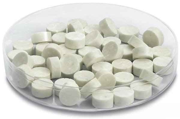
SnF₂ evaporation materials are typically supplied in the form of granules, powders, or pressed pellets, optimized for use in vacuum evaporation systems such as thermal evaporation or electron beam evaporation. Due to its relatively low decomposition temperature compared to oxide ceramics, SnF₂ requires careful process control to ensure stable evaporation and consistent film composition.
One of the key advantages of SnF₂ lies in its ability to introduce fluorine into deposited films, which can significantly influence refractive index, electrical behavior, and chemical resistance. In optical coatings, fluoride-based materials are valued for their low absorption and tailored refractive indices, making them suitable for multilayer interference coatings.
High-purity SnF₂ is essential to avoid contamination and ensure reproducible film performance. Additionally, controlled particle size and density help minimize spitting and ensure smooth deposition rates. In some applications, SnF₂ may be co-evaporated with other materials to achieve specific film compositions or doping effects.
Key features include:
Fluorine-containing compound for functional thin films
Suitable for thermal and e-beam evaporation processes
Enables tuning of optical and electrical film properties
Controlled particle size for stable evaporation behavior
Available in powder, granule, or pellet form
Applications
Tin(II) Fluoride evaporation materials are used in:
Optical coatings (low-index and fluoride-based multilayers)
Thin film electronics and functional coatings
Surface passivation and protective layers
Research in fluoride-based thin film materials
Specialized coatings requiring fluorine incorporation
Technical Parameters
| Parameter | Typical Value / Range | Importance |
|---|---|---|
| Chemical Formula | SnF₂ | Defines material composition |
| Purity | 99.9% – 99.99% | Ensures film consistency |
| Form | Powder / Granules / Pellets | Compatible with evaporation sources |
| Particle Size | 1 – 5 mm (granules typical) | Affects evaporation stability |
| Density | ≥ 95% theoretical (pressed forms) | Improves deposition uniformity |
| Evaporation Method | Thermal / E-beam | Determines process compatibility |
Comparison with Related Materials
| Material | Key Advantage | Typical Application |
|---|---|---|
| SnF₂ | Fluorine incorporation capability | Optical & functional films |
| MgF₂ | Very low refractive index | Anti-reflective coatings |
| AlF₃ | High transparency in UV range | Optical coatings |
| SnO₂ | Conductive oxide | Transparent electrodes |
FAQ
| Question | Answer |
|---|---|
| Is SnF₂ stable during evaporation? | It requires controlled conditions to prevent decomposition and ensure consistent film composition. |
| What form is recommended for use? | Granules or pressed pellets are preferred for stable evaporation. |
| Can it be co-evaporated with other materials? | Yes, it is often used in combination with other materials to tailor film properties. |
| Is it suitable for optical coatings? | Yes, especially for fluoride-based multilayer coatings. |
| Which industries use SnF₂ evaporation materials? | Optics, electronics, and advanced materials research. |
Packaging
Our Tin(II) Fluoride Evaporation Materials are meticulously tagged and labeled externally to ensure efficient identification and maintain high standards of quality control. We take great care to prevent any potential damage during storage and transportation, ensuring the materials arrive in perfect condition.
Conclusion
Tin(II) Fluoride (SnF₂) evaporation materials provide a versatile solution for producing fluorine-containing thin films with tailored optical and functional properties. With flexible forms, high purity, and compatibility with vacuum deposition systems, they are well-suited for advanced coating technologies and research applications.
For detailed specifications and a quotation, please contact us at sales@thinfilmmaterials.com


Reviews
There are no reviews yet.