Introduction
Tin Telluride (SnTe) sputtering targets are key materials for depositing IV–VI semiconductor thin films with unique electronic and optical properties. As a narrow bandgap semiconductor and a well-known topological crystalline insulator, SnTe is widely used in infrared devices, thermoelectric materials, and emerging quantum electronics. High-quality SnTe sputtering targets enable precise control over film composition and structure, which is critical for advanced functional thin films.
Detailed Description
Tin Telluride sputtering targets are typically produced with controlled stoichiometry (Sn:Te ≈ 1:1) using vacuum melting or hot pressing techniques to ensure high density and compositional uniformity. Maintaining the correct stoichiometric balance is essential, as deviations can significantly affect electrical conductivity, carrier concentration, and optical absorption properties.
SnTe exhibits a narrow bandgap (~0.18 eV at room temperature), making it highly suitable for infrared detection and thermoelectric applications. Its crystalline structure supports interesting electronic behaviors, including topological surface states, which are of increasing interest in next-generation electronics and spintronics.
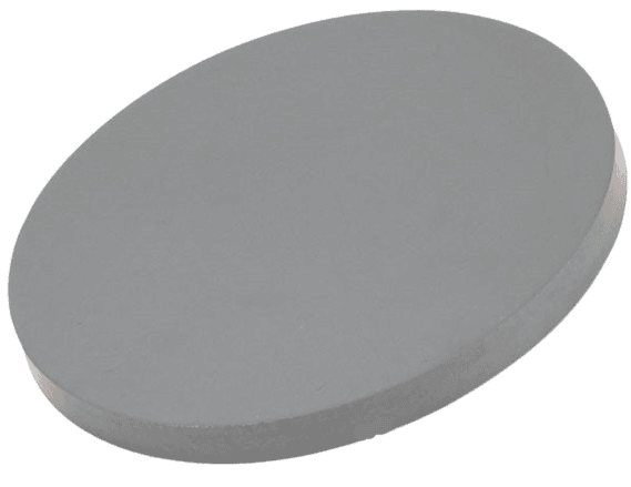
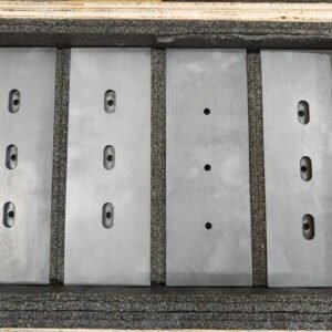
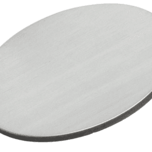
Due to the relatively high vapor pressure of tellurium, careful processing and sputtering control are required to maintain film composition. High-density targets help reduce preferential sputtering and improve film uniformity. Targets can be supplied as planar or rotatable designs and are often bonded to copper backing plates to enhance thermal conductivity and mechanical stability during deposition.
Key features include:
Precise stoichiometry control for consistent semiconductor properties
High density and uniform microstructure for stable sputtering
Suitable for RF and DC magnetron sputtering systems
Optimized for infrared and thermoelectric thin films
Custom sizes, purities, and bonding configurations available
Applications
Tin Telluride sputtering targets are widely used in:
Infrared detectors and imaging systems
Thermoelectric devices for energy conversion
Topological insulator research and quantum materials
Semiconductor thin films and electronic devices
Optical coatings in the infrared region
Advanced R&D in condensed matter physics
Technical Parameters
| Parameter | Typical Value / Range | Importance |
|---|---|---|
| Composition | SnTe (Sn:Te ≈ 1:1) | Determines semiconductor properties |
| Purity | 99.9% – 99.99% | Reduces impurities affecting performance |
| Density | ≥ 95% – 99% theoretical | Improves sputtering stability |
| Diameter | 25 – 200 mm (custom) | Fits sputtering systems |
| Thickness | 3 – 6 mm | Influences target lifetime |
| Bonding | Copper backing (In / elastomer) | Enhances heat dissipation |
| Sputtering Method | RF / DC magnetron | Process compatibility |
Comparison with Related Materials
| Material | Key Advantage | Typical Application |
|---|---|---|
| SnTe | Narrow bandgap, topological properties | IR devices, thermoelectrics |
| PbTe | High thermoelectric efficiency | Thermoelectric modules |
| SnSe | Exceptional thermoelectric performance | Energy conversion |
| GeTe | Phase-change and semiconductor behavior | Memory devices |
FAQ
| Question | Answer |
|---|---|
| Can the stoichiometry be adjusted? | Yes, slight adjustments can be made depending on application requirements. |
| What sputtering method is recommended? | RF sputtering is commonly used for compound semiconductors like SnTe. |
| Is bonding required? | For high-power sputtering, bonding to a copper backing plate is recommended. |
| What are the key challenges in deposition? | Maintaining stoichiometry due to tellurium volatility requires optimized sputtering parameters. |
| Which industries use SnTe targets most? | Semiconductor, infrared technology, and advanced materials research. |
Packaging
Our Tin Telluride Sputtering Targets are meticulously tagged and labeled externally to ensure efficient identification and maintain high standards of quality control. We take great care to prevent any potential damage during storage and transportation, ensuring the targets arrive in perfect condition.
Conclusion
Tin Telluride sputtering targets provide a reliable platform for depositing advanced semiconductor thin films with unique electronic and optical properties. With precise composition control and customizable configurations, they are ideal for infrared technologies, thermoelectric devices, and cutting-edge research applications.
For detailed specifications and a quotation, please contact us at sales@thinfilmmaterials.com.

Reviews
There are no reviews yet.