
 MSDS File
Product Overview
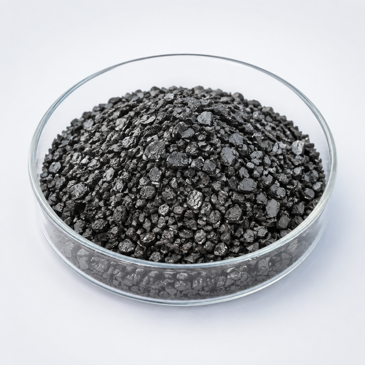
Titanium Diselenide Evaporation Materials (TiSe2) is a chalcogenide evaporation material used in optical, infrared, semiconductor, thermoelectric, and phase-change thin-film research. Because sulfur-, selenium-, and tellurium-containing compounds can contain volatile constituents, evaporation may be incongruent and the deposited film can deviate from the nominal source composition. Deposition temperature, source heating profile, rate control, and film-composition analysis are therefore important when stoichiometry is critical.
Evaporation Behavior and Process Considerations
Chalcogenides often contain constituents with different vapor pressures, so the film composition may evolve during evaporation. Lower source temperatures and controlled rates can help reduce loss of volatile components, but the optimum method depends on the specific compound. When stoichiometry is critical, deposited-film composition should be verified rather than inferred only from the source label.
Technical Data
| Material Type | Titanium diselenide |
| Symbol | TiSe2 |
| Appearance/Color | Dark brown |
| Molecular Weight | 205.81 |
| Structure | Octahedral |
| Purity | 99.9% ~ 99.99% |
| Shape | Powder/ Granule/ Custom-made |
Typical Thin-Film Applications
- Infrared, optical, phase-change, semiconductor, and thermoelectric thin films
- Compound semiconductor and chalcogenide multilayer research
- Composition-sensitive R&D where volatile-element control is important
Source Form and Ordering Considerations
For quotation, provide the material or formula, purity, desired source form and size, quantity, evaporation method if known, and any crucible, boat, or e-beam hearth constraints. For compound materials, include the target film composition or application when possible so that source form and process risk can be reviewed together. TFM can supply pellets, pieces, granules, tablets, or other custom forms subject to material manufacturability.
Frequently Asked Questions
Can Titanium Diselenide evaporate incongruently?
Yes. Sulfur, selenium, and tellurium compounds can contain constituents with different vapor pressures, so the deposited film may not exactly match the nominal source composition.
How can volatile-component loss be reduced when evaporating Titanium Diselenide?
A controlled source temperature, stable deposition rate, and appropriate substrate temperature can help. The optimum conditions depend on the specific compound and should be confirmed by film analysis.
Is thermal or e-beam evaporation better for Titanium Diselenide?
The better method depends on vapor pressure, decomposition temperature, source form, and desired rate. Some chalcogenides can be thermally evaporated, while others are more controllable with localized e-beam heating.
Should Titanium Diselenide film composition be measured after deposition?
Yes when stoichiometry is important. Source composition alone does not guarantee film composition because preferential evaporation and re-evaporation can occur.
What source form can TFM supply for Titanium Diselenide?
Depending on the material, TFM can review pellets, pieces, granules, or other compact forms suitable for the customer’s evaporation source.
What should I include in a Titanium Diselenide RFQ?
Provide composition, purity, source form and size, quantity, evaporation method, and the film-composition or application requirements that matter to the project.
Reviews
There are no reviews yet.