Titanium Silicon Sputtering Target Description
The Titanium Silicon Sputtering Target is a high-performance material, known for its high purity, density, sputtering rate, and strong adhesion. It also boasts excellent mechanical properties and low resistivity, making it an ideal choice for producing high-quality sputtered films. These films find widespread use in electronics, optics, chemistry, automotive, aerospace, and medical industries. The target’s high purity ensures that the resulting sputtered films are both pure and highly conductive, while its high density minimizes pores and impurities, enhancing the films’ density and stability. Additionally, Titanium Silicon Sputtering Targets possess excellent mechanical strength, allowing them to withstand energetic particle impacts and high-temperature environments. The low resistivity of these targets improves current transfer efficiency and reduces energy loss. These exceptional properties make Titanium Silicon Sputtering Targets a critical material for supporting various high-tech applications with reliability and precision.
Related Product: Aluminum Silicon Sputtering Target, Silicon Carbide Sputtering Target
Titanium Silicon Sputtering Target Specifications
| Compound Formula | Ti-Si |
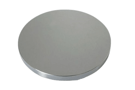
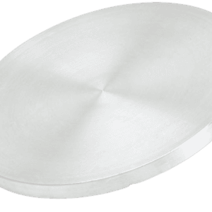
| Appearance | Silver Metallic Target |
| Melting Point | – |
| Density | 4.37 |
| Available Sizes | Dia.: 1.0″, 2.0″, 3.0″, 4.0″, 5.0″, 6.0″ Thick: 0.125″, 0.250″ |
Titanium Silicon Sputtering Target Handling Notes
Indium bonding is highly recommended for the Titanium Silicon Sputtering Target due to certain characteristics that make it challenging for direct sputtering, such as its brittleness and low thermal conductivity. These properties make the material susceptible to thermal shock, further emphasizing the need for proper bonding to ensure optimal performance during the sputtering process.
Titanium Silicon Sputtering Target Application
Titanium Silicon Sputtering Targets are versatile materials used across various industries, including electronics, optics, chemistry, automotive, aerospace, and medicine.
Electronics: These targets are essential in producing electronic components such as thin film resistors, capacitors, and transistors.
Optics: In the optics field, Titanium Silicon Sputtering Targets are utilized to create optical components like mirrors, windows, and gratings.
Chemistry: They are employed in the chemical industry to manufacture equipment like chemical reactors and reaction towers.
Automotive: Titanium Silicon Sputtering Targets play a crucial role in producing automotive components, including engine parts, transmission systems, and structural body parts.
Aerospace: In aerospace, these targets are used to fabricate aircraft and spacecraft components, such as engine parts and solar panels for spacecraft.
Medical: The medical industry benefits from Titanium Silicon Sputtering Targets in the production of medical devices and equipment, including surgical instruments, diagnostic tools, and pharmaceutical machinery.
Titanium Silicon Sputtering Target Packaging
We take great care in handling our Titanium Silicon Sputtering Target during storage and transportation to ensure it maintains its original quality and condition.
Get Contact
TFM offers Titanium Silicon Sputtering Targets in a variety of forms, purities, and sizes. We specialize in producing high-purity physical vapor deposition (PVD) materials with maximum density and minimal average grain sizes, making them ideal for use in semiconductor applications, chemical vapor deposition (CVD), and PVD processes for display and optical technologies.


Reviews
There are no reviews yet.