
 MSDS File
Tungsten Ditelluride Evaporation Materials Overview
Tungsten ditelluride, with the chemical formula WTe₂, is a specialized evaporation material utilized in various deposition techniques. Known for its high-purity, TFM offers tungsten ditelluride materials that are crucial for achieving superior quality in thin film deposition processes. Our commitment to excellence ensures that these materials meet up to 99.9995% purity, delivering reliable and consistent performance for your needs.
Specifications of Tungsten Ditelluride Evaporation Materials
| Material Type | Tungsten Ditelluride |
| Symbol | WTe2 |
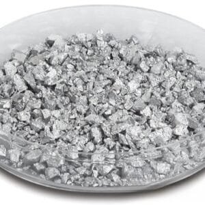
| Appearance/Color | Gray crystals |
| Melting Point | 1,020 °C (1,870 °F; 1,290 K) |
| Density | 9.43 g/cm3 |
| Purity | 99.9% ~ 99.999% |
| Shape | Powder/ Granule/ Custom-made |
Applications of Tungsten Ditelluride Evaporation Materials
Tungsten ditelluride evaporation materials are integral to various deposition methods, including:
- Semiconductor Deposition: Essential for producing high-performance semiconductor devices.
- Chemical Vapor Deposition (CVD): Used for creating thin films in a controlled environment.
- Physical Vapor Deposition (PVD): Ideal for applications requiring precise coating.
- Optical Coatings: Employed in wear-resistant coatings, decorative finishes, and display technologies.
Packaging and Handling
Our tungsten ditelluride evaporation materials are meticulously packaged in vacuum-sealed plastic bags to ensure their integrity during storage and shipping. Each package includes a Certificate of Analysis (COA) to verify the quality and purity of the material.
Contact Us
At TFM, we pride ourselves on our advanced engineering and manufacturing capabilities. Our tungsten ditelluride evaporation materials are designed to meet the highest industry standards for use in a variety of applications, from semiconductors to optical coatings. For more information or to request a quote, please reach out to us today.


Reviews
There are no reviews yet.