
Tungsten Selenide Sputtering Target
The Tungsten Selenide (WSe₂) Sputtering Target from Thin Film Materials (TFM) is a high-purity compound sputtering material widely used in semiconductors, optoelectronics, and energy devices. Tungsten selenide is a member of the transition metal dichalcogenide (TMD) family, known for its layered crystal structure and tunable electronic and optical properties. When fabricated into sputtering targets, WSe₂ enables the deposition of uniform thin films that are essential for advanced research and device engineering.
Detailed Description
WSe₂ sputtering targets are engineered to deliver high density, uniform grain size, and exceptional film quality. With typical purities ranging from 99.9% (3N) to 99.99% (4N), they provide excellent control of stoichiometry and minimize film contamination.
Chemical Formula: WSe₂
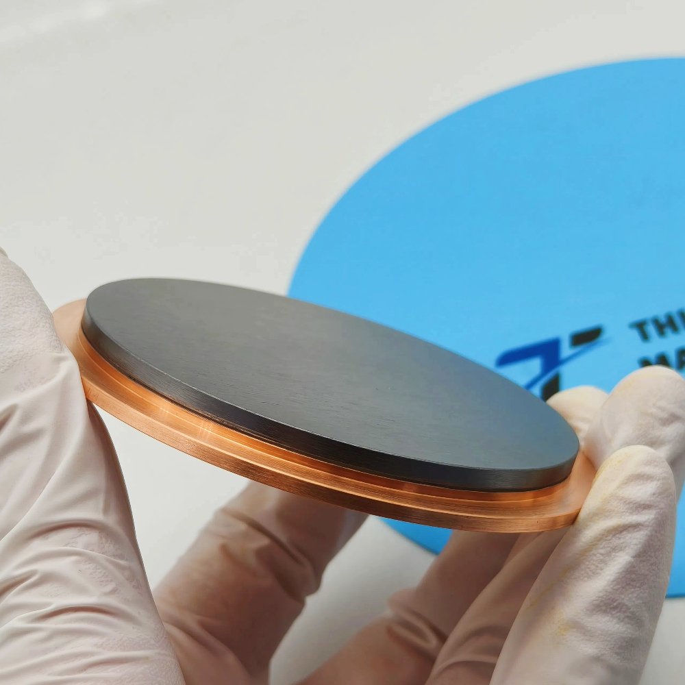
Appearance: Dark gray to black crystalline solid
Crystal Structure: Hexagonal layered structure (similar to MoS₂)
Density: ~9.32 g/cm³
Melting Point: ~1,550 °C (decomposes before melting in air)
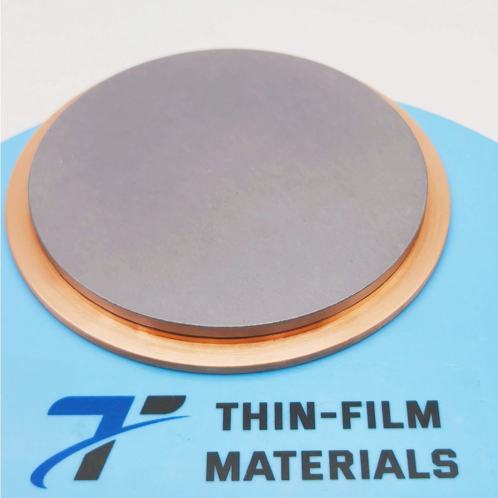
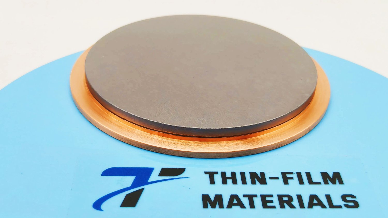
TFM supplies WSe₂ sputtering targets in disc, rectangular, and step target formats. Bonding services with copper or titanium backing plates are available to improve thermal management and mechanical stability during deposition. Custom shapes and dimensions can be provided upon request.
Applications
Tungsten Selenide sputtering targets are widely applied in:
Semiconductors: 2D materials for transistors, FETs, and integrated circuits
Optoelectronics: thin films for photodetectors, LEDs, and sensors
Solar energy: absorber layers in next-generation photovoltaic devices
Thermoelectrics: thin films for energy conversion and heat management
Research: advanced studies on layered TMDs for quantum and nanoelectronics
Technical Parameters
| Parameter | Typical Value / Range | Importance |
|---|---|---|
| Purity | 99.9% – 99.99% | Ensures high film quality and stability |
| Diameter | 25 – 150 mm (custom up to 300 mm) | Compatible with most sputtering systems |
| Thickness | 3 – 6 mm | Controls sputtering rate and uniformity |
| Bonding Options | Indium / Elastomer | Improves adhesion and thermal stability |
| Backing Plate | Copper / Titanium | Provides better heat dissipation and durability |
Comparison with Related Materials
| Material | Key Advantage | Typical Application |
|---|---|---|
| WSe₂ | Layered 2D semiconductor properties | Transistors, solar cells, optoelectronics |
| MoS₂ | High electron mobility | Electronics, lubrication films |
| WS₂ | Strong mechanical & optical stability | Optoelectronics, photonics |
FAQ
| Question | Answer |
|---|---|
| Can WSe₂ sputtering targets be customized? | Yes, TFM offers custom diameters, thicknesses, purity levels, and bonding options. |
| Do you provide bonded targets? | Yes, indium and elastomer bonding are available for enhanced durability and performance. |
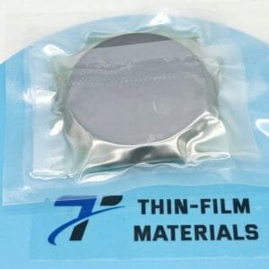
| How are WSe₂ targets packaged? | Each target is vacuum-sealed, cushioned with foam, and shipped in export-safe cartons or crates. |
| Which industries use WSe₂ targets most? | Semiconductor, photovoltaic, sensor, and advanced R&D fields. |
Packaging
All Tungsten Selenide sputtering targets are vacuum-sealed and securely packaged to prevent oxidation, moisture exposure, and mechanical damage. Export-safe cartons or wooden crates are used to ensure safe transport.
Conclusion
The Tungsten Selenide (WSe₂) Sputtering Target from TFM provides high purity, reliable performance, and customizable options for thin film deposition. With its unique layered structure and tunable properties, WSe₂ is a critical material for next-generation electronics, energy, and photonic devices.
For detailed specifications, quotations, and tailored solutions, please contact us at sales@thinfilmmaterials.com.

Reviews
There are no reviews yet.