
 MSDS File
Overview of Ytterbium Trifluoride Evaporation Materials
Ytterbium Trifluoride (YbF3), or Ytterbium Fluoride, is a crystalline ionic substance with minimal solubility in water. Its key applications include use in fluoride glass and optical film materials. Due to its high light transmittance and low refractive index across a broad spectrum—from ultraviolet to far infrared (0.2–15μm)—YbF3 is a preferred choice in the creation of mid-infrared multilayer films.
Specification of Ytterbium Trifluoride Evaporation Materials
| Chemical formula | YbF3 |
| Purity | 2N-4N |
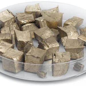
| Appearance | Granules |
| Melting point | 1157℃ |
| Formula weight | 230.04 |
| Size | 0.1-5mm or customized |
| Color | Light grey |
Applications of Ytterbium Trifluoride Evaporation Materials
Ytterbium Trifluoride is renowned for its wide transmission band, making it highly effective in the infrared range. It is utilized in various applications, including:
- Decorative Coatings: Enhances the aesthetic qualities of surfaces.
- UV Coatings: Provides protection and functionality in ultraviolet applications.
- Glass Coatings: Improves optical properties and durability of glass products.
Packaging
Our ytterbium fluoride evaporation materials are meticulously packaged in plastic vacuum bags to ensure protection during storage and transportation. This packaging maintains the integrity of the product and includes a Certificate of Analysis (COA) for verification of quality.
Contact Us
TFM is dedicated to delivering high-purity ytterbium fluoride evaporation materials for applications in semiconductors, chemical vapor deposition (CVD), and physical vapor deposition (PVD). Our strong engineering, manufacturing, and analytical teams work together to produce top-tier evaporation materials. Reach out to us today to inquire about our products.


Reviews
There are no reviews yet.