
 MSDS File
Product Overview
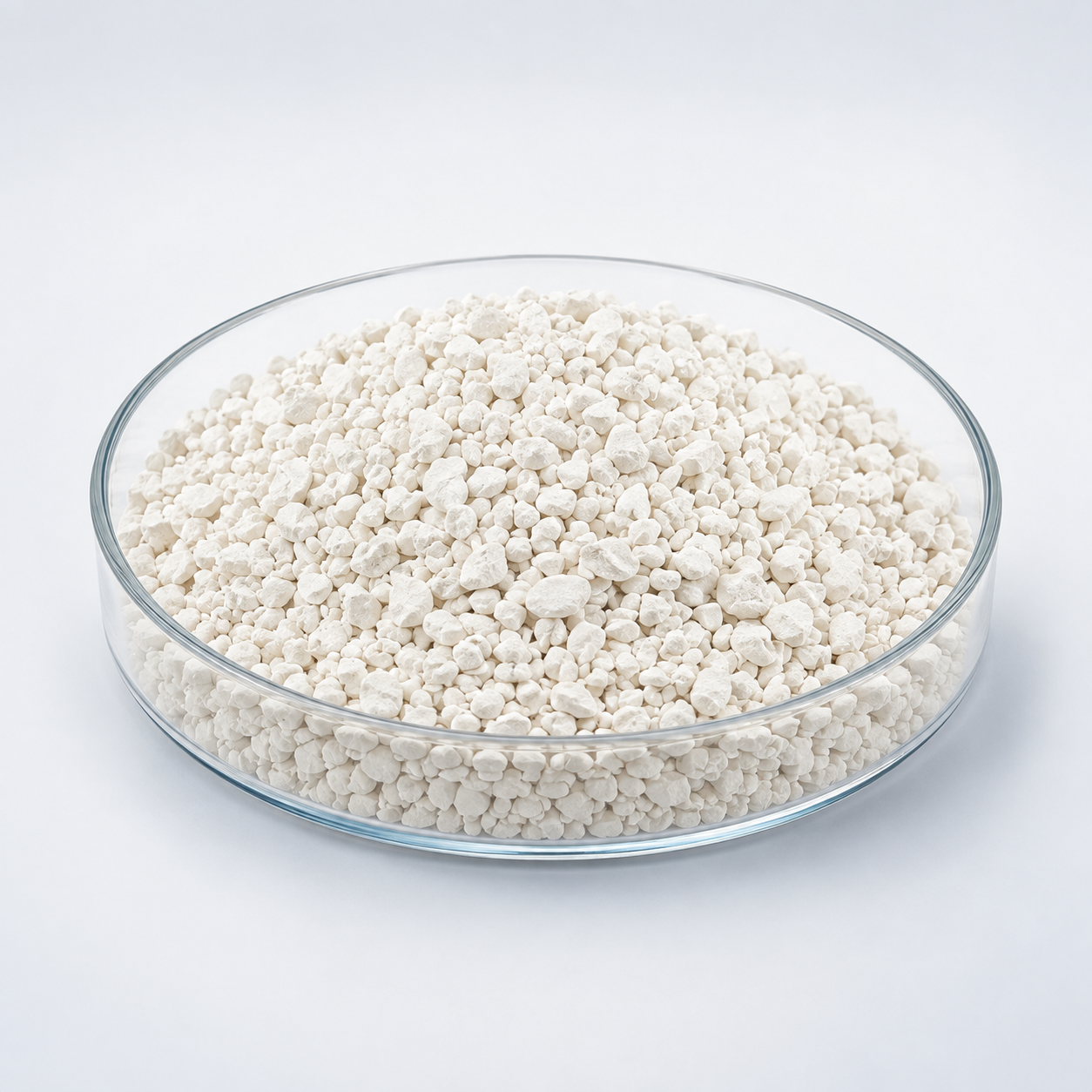
Ytterbium Oxide Evaporation Materials (Yb2O3) is a ceramic evaporation material for depositing oxide thin films used in optical, dielectric, electronic, magnetic, protective, or research applications. Many oxides have high melting temperatures and can partially dissociate or lose oxygen during evaporation, making electron-beam evaporation a common process option. Source density, pellet or piece geometry, crucible compatibility, oxygen background, deposition rate, and substrate conditions can all affect film stoichiometry and microstructure.
Evaporation Behavior and Process Considerations
Electron-beam evaporation is frequently evaluated for ceramic oxides because many have high melting temperatures. During heating, oxygen can be lost or the source can partially dissociate, so oxygen partial pressure, substrate temperature, deposition rate, and any post-deposition anneal may need optimization. The source should be conditioned gradually to minimize cracking, spitting, and sudden outgassing.
Technical Data
| Material Type | Ytterbium(III) Oxide |
| Symbol | Yb2O3 |
| Appearance/Color | White solid |
| Melting Point | 2,355 °C (4,271 °F; 2,628 K) |
| Density | 9.17 g/cm3, solid. |
| Purity | 99.9% ~ 99.99% |
| Shape | Powder/ Granule/ Custom-made |
Typical Thin-Film Applications
- Optical, dielectric, transparent conductive, magnetic, protective, or functional oxide films
- Displays, photovoltaics, sensors, semiconductors, and multilayer optical coatings where applicable
- Research on composition, oxygen content, phase, and post-deposition treatment
Source Form and Ordering Considerations
For quotation, provide the material or formula, purity, desired source form and size, quantity, evaporation method if known, and any crucible, boat, or e-beam hearth constraints. For compound materials, include the target film composition or application when possible so that source form and process risk can be reviewed together. TFM can supply pellets, pieces, granules, tablets, or other custom forms subject to material manufacturability.
Frequently Asked Questions
Is Ytterbium Oxide commonly evaporated by electron beam?
Electron-beam evaporation is frequently evaluated for high-melting ceramic oxides because it can provide localized heating. The exact method depends on the oxide, source form, and required film properties.
Can Ytterbium Oxide lose oxygen during evaporation?
Yes. Some oxides can partially dissociate or become oxygen-deficient under vacuum heating. Oxygen partial pressure, substrate temperature, deposition rate, and post-annealing can influence the final film composition.
Why can oxide evaporation sources spit or crack?
Rapid heating, trapped gas, porosity, and thermal gradients can cause cracking or particle ejection. A gradual conditioning ramp and stable source geometry help reduce these effects.
Does the deposited film always match the composition of Yb2O3?
Not always. Preferential evaporation, oxygen loss, decomposition, and substrate conditions can shift film chemistry or phase relative to the source material.
What source form is suitable for Ytterbium Oxide?
Pellets, tablets, pieces, or granules may be used depending on the e-beam pocket or crucible. A dense and mechanically stable source form is usually easier to condition reproducibly.
What information should I provide for a Ytterbium Oxide quotation?
Provide formula or composition, purity, source form and size, quantity, evaporation method, source-holder dimensions, and any film-composition or documentation requirements.
Reviews
There are no reviews yet.