Generic selectors
Exact matches only
Search in title
Search in content
Post Type Selectors

VD0590 Yttrium Evaporation Materials, Y

Material Type:Yttrium
Color/Appearance:Silvery White, Metallic
Purity:99.5% ~ 99.99%
Shape: Powder/ Granule/ Custom-made

TFM is a leading manufacturer and supplier of high-purity yttrium evaporation materials, along with a diverse range of other evaporation materials. We provide these materials in both powder and granule forms, and customized options are available upon request.

Yttrium Evaporation Materials Description

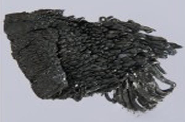
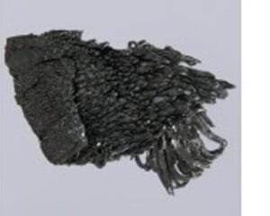
Yttrium, a gray-black metal with the chemical symbol Y, was the first rare earth metal to be discovered. It is ductile, reacts with hot water, and is readily soluble in dilute acids. Yttrium is used in the production of specialized glasses and alloys.

High-purity yttrium evaporation materials are crucial for ensuring high-quality film deposition. TFM specializes in producing yttrium evaporation materials with up to 99.99% purity, using rigorous quality assurance processes to ensure product reliability.

Yttrium Evaporation Materials Specification

Material TypeYttrium, Y
Density4.472 g·cm3
Color/AppearanceSilvery White, Metallic
Thermal Conductivity17.2 W/m.K
Melting Point1526 °C
Boiling Point3336 °C
Coefficient of Thermal Expansion10.6 x 10-6/K
Z Ratio0.835
SynonymsYttrium Pellets, Yttrium Pieces, Yttrium Evaporation Pellet, Y Pellets, Y Pieces, Y Evaporation Pellet

Yttrium Evaporation Materials Applications

  • Deposition Processes: Utilized in semiconductor deposition, chemical vapor deposition (CVD), and physical vapor deposition (PVD).
  • Optics: Applied in wear protection, decorative coatings, and displays.

Yttrium Evaporation Materials Packaging

Our yttrium evaporation materials are meticulously handled to avoid damage during storage and transportation, ensuring they maintain their original quality.

Contact Us

TFM offers yttrium evaporation materials in various forms, purities, sizes, and price ranges. We specialize in producing high-purity e-beam evaporation materials with optimal density and minimal average grain sizes. For current pricing on evaporation pellets and other deposition materials not listed, please contact us with your inquiry.

Reviews

There are no reviews yet.

Be the first to review “VD0590 Yttrium Evaporation Materials, Y”

Your email address will not be published. Required fields are marked *

FAQ

  • They are high‐purity substances (e.g. metals, alloys, or compounds) used in thermal or electron‐beam evaporation processes to form thin films on substrates.

  • Typically, they’re processed into a form (often ingots, pellets, or wires) that can be efficiently vaporized. Preparation emphasizes high purity and controlled composition to ensure film quality.

  • Thermal evaporation and electron-beam (e-beam) evaporation are the two main techniques, where material is heated (or bombarded with electrons) until it vaporizes and then condenses on the substrate.

  • Thermal evaporation heats the material directly (often using a resistive heater), while e-beam evaporation uses a focused electron beam to locally heat and vaporize the source material—each method offering different control and energy efficiency.

  • Key parameters include source temperature, vacuum level, deposition rate, substrate temperature, and the distance between the source and the substrate. These factors influence film uniformity, adhesion, and microstructure.

  • Evaporation generally produces high-purity films with excellent control over thickness, and it is especially suitable for materials with relatively low melting points or high vapor pressures.

  • Challenges include issues with step coverage (due to line-of-sight deposition), shadowing effects on complex topographies, and possible re-evaporation of material from the substrate if temperature isn’t properly controlled.

  • Common evaporation materials include noble metals (e.g., gold, silver), semiconductors (e.g., silicon, germanium), metal oxides, and organic compounds—each chosen for its specific optical, electrical, or mechanical properties.

  • Selection depends on desired film properties (conductivity, optical transparency, adhesion), compatibility with the evaporation process, and the final device application (semiconductor, optical coating, etc.).

  • Optimizing substrate temperature, deposition rate, and chamber vacuum are critical for ensuring that the film adheres well and forms the intended microstructure without defects.

  • Troubleshooting may involve checking the source material’s purity, ensuring stable source temperature, verifying the vacuum level, adjusting the substrate’s position or temperature, and monitoring deposition rate fluctuations.

While evaporation tends to yield very high purity films with excellent thickness control, it is limited by its line-of-sight nature. In contrast, sputtering can deposit films more uniformly on complex surfaces and is more versatile for a broader range of materials.


Shopping Cart
Scroll to Top