
 MSDS File
Introduction
Zinc Arsenic (ZnAs) Pellet Evaporation Material is a compound semiconductor source designed for controlled thin film deposition in advanced electronic and optoelectronic applications. As a zinc–arsenic system, ZnAs materials are primarily used in compound semiconductor research, doping processes, and specialized thin film structures where precise compositional control is critical.
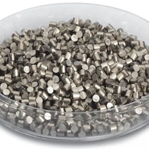
Supplied in pellet form, ZnAs evaporation materials enable stable feeding behavior and consistent evaporation rates in thermal or electron beam deposition systems. They are widely utilized in research laboratories and semiconductor development environments that require accurate stoichiometry and high material purity.
Detailed Description
Zinc and arsenic form several intermetallic and compound phases, and ZnAs evaporation materials are carefully synthesized to ensure controlled composition and phase stability. Maintaining the correct Zn:As ratio is essential, as deviations can significantly impact electrical properties, carrier concentration, and film uniformity.
ZnAs pellets are produced using high-purity zinc and arsenic raw materials through controlled alloying or compound synthesis processes under vacuum or inert atmospheres. Strict control of oxygen and moisture exposure is critical, particularly due to arsenic’s volatility and reactivity.
Pelletized form offers several advantages:
Improved loading efficiency in evaporation sources
More uniform heating compared to loose granules
Reduced splashing and spitting during thermal ramp-up
Better control of evaporation rate
ZnAs evaporation materials are compatible with:
Thermal evaporation (resistive heating)
Electron beam evaporation systems
Deposition parameters must be carefully optimized because arsenic has a relatively high vapor pressure. Controlled temperature ramping and chamber pressure management are recommended to ensure stoichiometric transfer and minimize preferential evaporation.
Typical deposited ZnAs-based films exhibit:
Controlled semiconductor behavior
Tunable carrier concentration
Compatibility with compound semiconductor structures
Stable interface formation with III–V and II–VI materials
Applications
Zinc Arsenic Pellet Evaporation Materials are commonly used in:
Compound Semiconductor Research – Zn–As thin film studies
Doping Processes – Controlled arsenic incorporation
Optoelectronic Devices – Specialized semiconductor layers
Thin Film Transistors (TFTs) – Experimental channel materials
Advanced Materials Research – Phase and band structure investigations
ZnAs materials are primarily used in research-scale and specialized semiconductor fabrication processes.
Technical Parameters
| Parameter | Typical Value / Range | Importance |
|---|---|---|
| Purity | 99.9% – 99.999% (metals basis) | Ensures controlled electrical behavior |
| Form | Pressed Pellets | Stable evaporation and loading efficiency |
| Composition | Stoichiometric ZnAs or custom ratio | Controls film properties |
| Pellet Diameter | 3 – 10 mm (custom available) | Matches evaporation crucibles |
| Melting Behavior | Controlled alloy phase | Supports uniform deposition |
| Deposition Method | Thermal / E-beam Evaporation | Suitable for semiconductor thin films |
Comparison with Related Materials
| Material | Key Advantage | Typical Application |
|---|---|---|
| ZnAs | Controlled Zn–As stoichiometry | Semiconductor research |
| ZnSe | Wide bandgap semiconductor | Optoelectronics |
| GaAs | Established III–V semiconductor | High-speed electronics |
| ZnTe | II–VI semiconductor with optical use | Photonic devices |
Compared to GaAs, ZnAs-based materials are typically used in more specialized or exploratory semiconductor research environments.
FAQ
| Question | Answer |
|---|---|
| Can the ZnAs composition be customized? | Yes, stoichiometry and pellet dimensions can be tailored to meet deposition requirements. |
| Is ZnAs suitable for thermal evaporation? | Yes, both resistive heating and e-beam systems are compatible with proper parameter control. |
| Are special handling precautions required? | Yes, due to arsenic content, appropriate safety and ventilation procedures are necessary during handling and deposition. |
| What industries use ZnAs evaporation materials? | Primarily semiconductor R&D laboratories and advanced materials research facilities. |
| How is the material packaged? | Vacuum-sealed packaging with moisture protection and secure export-grade containers. |
Packaging
Our Zinc Arsenic Pellet Evaporation Materials are meticulously tagged and labeled externally to ensure efficient identification and maintain high standards of quality control. We take great care to prevent any potential damage during storage and transportation, ensuring the materials arrive in perfect condition.
Conclusion
Zinc Arsenic Pellet Evaporation Material (ZnAs) provides a reliable and customizable solution for semiconductor thin film deposition and advanced research applications. With controlled composition, high purity, and stable pellet form, ZnAs supports precise material engineering in compound semiconductor systems.
For detailed specifications and a quotation, please contact us at sales@thinfilmmaterials.com.


Reviews
There are no reviews yet.