
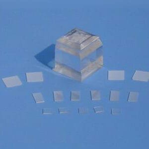
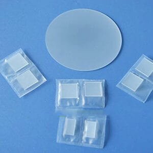
TFM Zinc Oxide (ZnO) Substrate
TFM offers high-quality Zinc Oxide (ZnO) substrates, ideal for GaN film growth and widely used in optoelectronics, UV devices, and high-temperature electronics. ZnO features a 3.73 eV band-gap with a 60 meV exciton binding energy at room temperature, making it an exceptional material for ultraviolet and visible light luminescence.
Zinc Oxide Substrate Physical Properties
| Property | Details |
|---|---|
| Material | ZnO |
| Growth Method | MOCVD |
| Crystal Structure | Hexagonal |
| Lattice (Å) | a = 3.252, c = 5.313 |
| Direction | <0001> 3.5º |
| Density (g/cm³) | 5.7 g/cm³ |
| Hardness (Mohs) | 4.0 |
| Melting Point | 1975°C |
| Thermal Expansion Coefficient (CTE) | 6.5 x 10⁻⁶ /°C along a axis, 3.7 x 10⁻⁶ /°C along c axis |
| Seebeck Coefficient | 1200 μV/K @ 300°C |
| Thermal Conductivity | 0.006 Cal/cm·K |
| Optical Transmission | > 50% for 2 mm thickness (wavelength 400 nm ~ 600 nm) |
Zinc Oxide Substrate Specifications
| Specification | Details |
|---|---|
| Size | 25x25x0.5 mm, 10x10x0.5 mm, 10x5x0.5 mm, 5x5x0.5 mm |
| Thickness | 0.5 mm |
| Crystal Orientation | <0001>, <11-20>, <10-10> |
| Polished | SSP or DSP |
| Redirection Precision | ±0.5° |
| Edge Redirection | 2° (special in 1°) |
| Angle of Crystalline | Special sizes and orientations available upon request |
| Surface Roughness (Ra) | ≤ 5 Å (5 μm × 5 μm) |
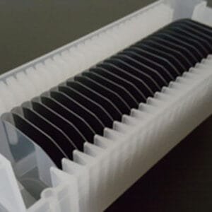
Zinc Oxide Substrate Packaging
TFM ensures that all Zinc Oxide substrates are carefully packaged in a class 100 clean bag or wafer container within a class 1000 clean room, ensuring maximum protection during transport.
Opt for TFM’s Zinc Oxide substrates for high-performance applications in optoelectronics and UV devices, offering superior material properties for your advanced semiconductor needs.
Reviews
There are no reviews yet.