
Introduction
Zinc Oxysulfide (ZnOS) Sputtering Target is a specialized material widely used in thin-film deposition, especially for optoelectronic and semiconductor research. With its tunable optical and electronic properties, ZnOS enables precise control over film characteristics, making it valuable in solar cells, transparent conductive films, and advanced coating technologies.
Detailed Description
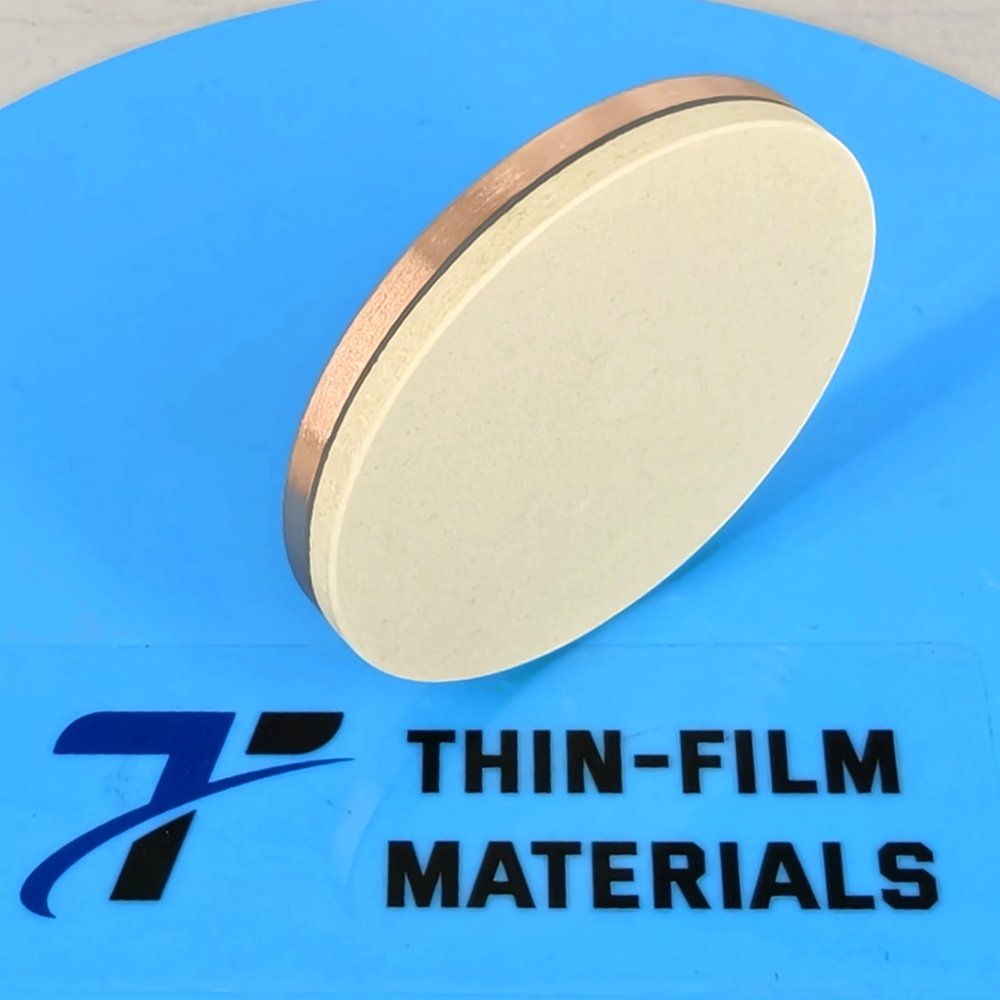
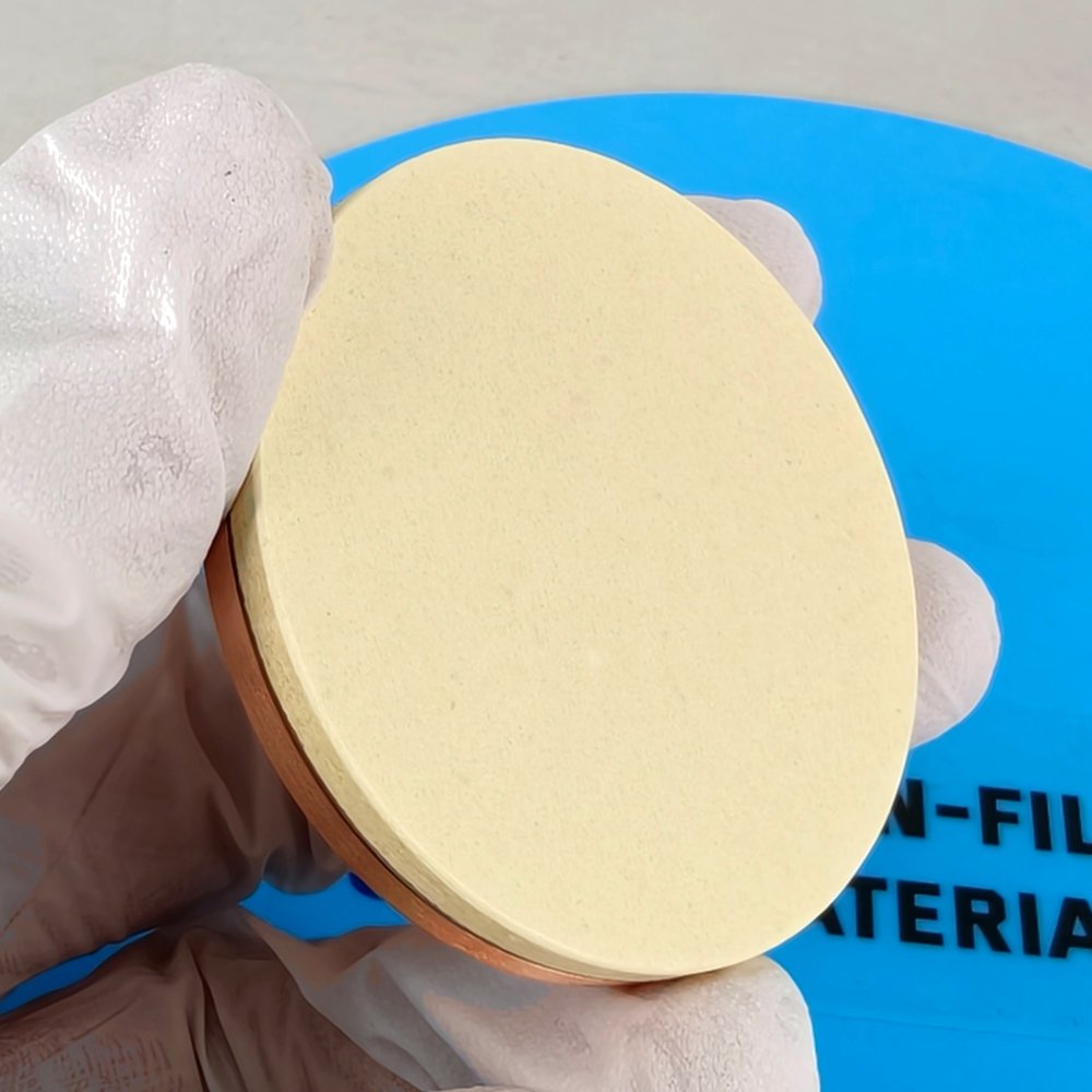
The Zinc Oxysulfide Sputtering Target is typically produced by high-purity powder synthesis followed by densification techniques such as hot pressing or vacuum sintering. The material offers a unique combination of zinc, oxygen, and sulfur elements, giving it adjustable bandgap properties between ZnO and ZnS. This versatility allows researchers and manufacturers to tailor thin-film performance for specific device requirements.
Key characteristics include:
High Purity (3N–4N, 99.9–99.99%), ensuring minimal contamination during deposition.
Uniform Microstructure, which contributes to stable sputtering rates and consistent thin-film thickness.
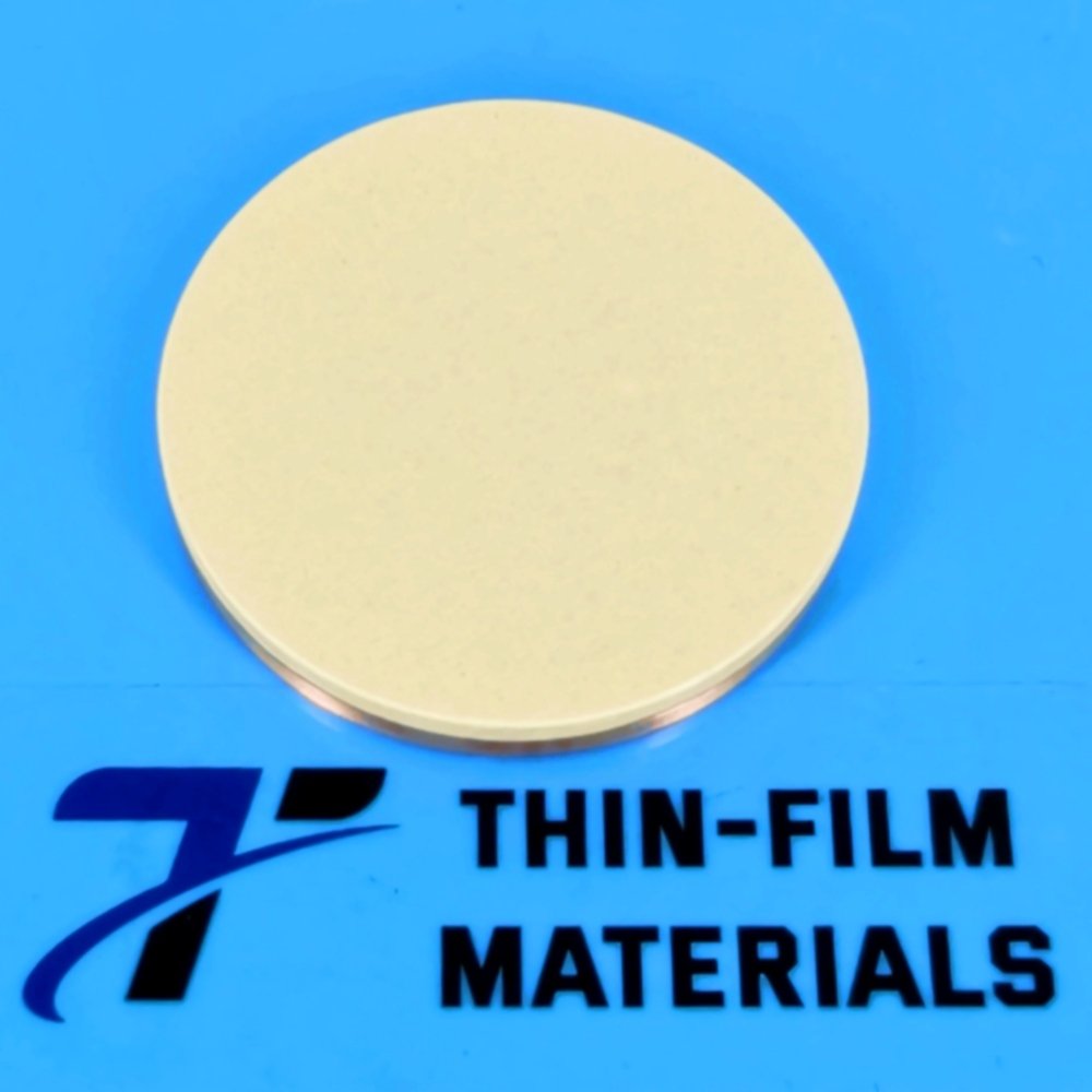
Customizable Geometry, available in discs, rectangular plates, or step targets for different sputtering systems.
Bonding Options, such as copper or indium bonding, to improve thermal conductivity and mechanical stability during sputtering.
Applications
Zinc Oxysulfide Sputtering Targets are used across multiple industries:
Photovoltaics – buffer and window layers in thin-film solar cells.
Optoelectronics – LED structures and photodetectors requiring controlled bandgap properties.
Transparent Conductive Films – for displays, touch panels, and energy-efficient windows.
Research & Development – material science and semiconductor device prototyping.
Technical Parameters
| Parameter | Typical Value / Range | Importance |
|---|---|---|
| Purity | 99.9% – 99.99% (3N–4N) | High purity ensures defect-free films |
| Diameter | 25 – 300 mm (customizable) | Fits standard sputtering systems |
| Thickness | 3 – 10 mm | Affects sputtering rate and lifetime |
| Bonding | Indium / Copper backing | Enhances heat transfer and stability |
Comparison with Related Materials
| Material | Key Advantage | Typical Application |
|---|---|---|
| ZnOS | Tunable bandgap, improved film control | Solar cells, transparent coatings |
| ZnO | High transparency, conductivity | Display technologies |
| ZnS | Wide bandgap, optical applications | Optics and photonics |
FAQ
| Question | Answer |
|---|---|
| Can the ZnOS target be customized? | Yes, diameter, thickness, purity, and bonding can be tailored to your system. |
| How is the product packaged? | Vacuum-sealed with foam protection, shipped in export-grade cartons or wooden crates. |
| What industries use ZnOS most? | Solar energy, optoelectronics, display manufacturing, and advanced R&D. |
| Does ZnOS improve solar cell efficiency? | Yes, its tunable bandgap enables better light absorption and conversion efficiency. |
Packaging
Our Zinc Oxysulfide Sputtering Targets are carefully vacuum-packed and externally labeled to ensure traceability and protection. Each target is cushioned with shock-absorbing foam and shipped in export-compliant cartons or wooden crates to prevent damage during transit.
Conclusion
Zinc Oxysulfide Sputtering Target offers unique optical and electronic flexibility, making it an excellent choice for cutting-edge thin-film technologies. With high purity, stable performance, and customizable specifications, it supports a wide range of industrial and research applications.
For detailed specifications or a quotation, please contact us at sales@thinfilmmaterials.com.


Reviews
There are no reviews yet.