Introduction
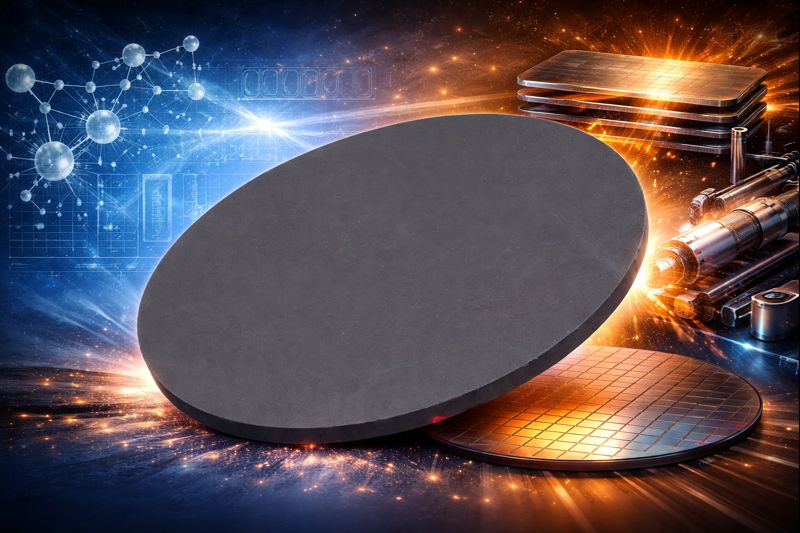
Samarium Nickel Oxide sputtering targets—commonly represented by compositions such as SmNiO₃ or related samarium–nickelate oxide phases—belong to a class of complex oxide materials that have attracted increasing attention in recent years. These materials sit at the intersection of strongly correlated electron systems, oxide electronics, and functional thin-film technologies.
Unlike conventional metallic or simple oxide sputtering targets, samarium nickel oxide targets are primarily used to deposit functional oxide thin films whose electrical, optical, and structural properties are highly sensitive to stoichiometry, crystallinity, and deposition conditions. As a result, their value lies not in volume consumption but in enabling advanced device concepts that cannot be realized using traditional materials.
This article provides a detailed, application-focused analysis of samarium nickel oxide sputtering targets, explaining why these targets are used, what types of thin films they enable, and which industries and research fields depend on them.
1. Background: Samarium Nickel Oxide as a Functional Oxide System
1.1 Material Classification and Crystal Structure
Samarium nickel oxide is part of the rare-earth nickelate (RNiO₃) family, where R represents a rare-earth element such as La, Nd, Sm, or Pr. These materials typically adopt a perovskite-related crystal structure, with strong coupling between lattice, charge, and electronic degrees of freedom.
Sm-based nickelates are particularly interesting because:
- Samarium has a relatively small ionic radius compared to La or Nd
- This leads to stronger lattice distortion
- The distortion directly affects electron bandwidth and transport behavior
As a result, SmNiO₃ and related compositions show highly tunable electronic properties, making them ideal candidates for next-generation oxide electronics.
1.2 Why Use a Sputtering Target?
To exploit these properties in real devices, samarium nickel oxide must be deposited as uniform, compositionally controlled thin films. Magnetron sputtering—using ceramic samarium nickel oxide targets—offers:
- Precise control of film thickness
- Good uniformity over large substrates
- Compatibility with semiconductor and oxide device fabrication
This makes sputtering targets the preferred form for both research-scale and pilot-scale production of samarium nickel oxide thin films.
2. Oxide Electronics and Neuromorphic Devices
2.1 Metal–Insulator Transition (MIT) Behavior
One of the most important application drivers for samarium nickel oxide thin films is their temperature- and field-driven metal–insulator transition (MIT). SmNiO₃ exhibits a sharp and reversible change in electrical conductivity under external stimuli such as:
- Temperature
- Electric field
- Strain or pressure
This transition is a hallmark of strongly correlated electron materials and is central to many emerging device concepts.
2.2 Neuromorphic and Brain-Inspired Computing
In neuromorphic electronics, materials that can emulate synaptic behavior are highly sought after. Samarium nickel oxide thin films deposited from sputtering targets are actively studied for:
- Artificial synapses
- Memristive devices
- Adaptive and learning circuits
Key advantages include:
- Analog tunability of resistance
- Non-volatile or semi-volatile switching behavior
- Compatibility with oxide heterostructures
In this context, the stoichiometric accuracy and density of the sputtering target are critical, as even small deviations can significantly alter switching behavior.
3. Thin-Film Transistors and Oxide Semiconductor Research
3.1 Channel and Functional Layers
While samarium nickel oxide is not a conventional wide-bandgap semiconductor like IGZO, it is increasingly used as:
- A functional channel layer
- A modulating layer in oxide transistor stacks
- A correlated oxide layer coupled with conventional semiconductors
Sputtered Sm–Ni–O films allow researchers to explore new transistor architectures that go beyond purely charge-based operation.
3.2 Interface Engineering
Samarium nickel oxide is particularly valuable in interface engineering, where its strong electron–lattice coupling can influence:
- Carrier mobility at interfaces
- Threshold voltage behavior
- Interfacial phase transitions
These studies rely heavily on high-quality sputtering targets that ensure reproducible film composition and smooth surface morphology.
4. Sensors and Smart Functional Devices

4.1 Temperature and Gas Sensors
Due to its strong sensitivity to temperature and ambient atmosphere, samarium nickel oxide thin films are investigated for:
- High-temperature resistive sensors
- Gas sensing devices for oxidizing or reducing environments
The MIT behavior and oxygen stoichiometry sensitivity make Sm–Ni–O films particularly responsive to environmental changes.
4.2 Adaptive and Self-Regulating Systems
In smart systems research, samarium nickel oxide films are explored as:
- Self-regulating resistive elements
- Components in adaptive circuits that respond dynamically to external stimuli
These applications benefit from the fast response and reversibility of property changes in Sm–Ni–O thin films.
5. Energy-Related Applications and Electrochemical Devices
5.1 Electrodes for Advanced Energy Systems
Although not as widely used as cobalt or manganese oxides, samarium nickel oxide is being studied as:
- A functional electrode material
- A catalytic or pseudocapacitive layer in electrochemical devices
Its mixed ionic–electronic conductivity and chemical stability under certain conditions make it attractive for exploratory energy research.
5.2 Solid-State and Thin-Film Energy Devices
In thin-film batteries and solid-state electrochemical systems, sputtered Sm–Ni–O layers can serve as:
- Model electrode materials
- Interface modification layers to control charge transport
Again, film quality is directly linked to the phase purity and density of the sputtering target.
6. Optical and Optoelectronic Research
6.1 Optical Modulation and Switching
Samarium nickel oxide exhibits changes in optical properties—such as reflectivity and absorption—across its metal–insulator transition. Thin films deposited from sputtering targets are therefore studied for:
- Optical switching devices
- Thermochromic and electrochromic systems
These effects are particularly relevant in mid-infrared and near-infrared regimes, where correlated oxides offer tunable responses.
6.2 Integrated Oxide Photonics
In integrated photonic platforms, Sm–Ni–O films can be used as:
- Active modulation layers
- Functional coatings on waveguides
Such applications demand smooth, dense, and compositionally uniform films, reinforcing the importance of high-quality sputtering targets.
7. Fundamental Research in Strongly Correlated Materials
7.1 Model System for Correlated Electron Physics
Samarium nickel oxide is widely regarded as a model system for studying:
- Electron correlation effects
- Coupling between lattice distortion and electronic transport
- Strain-induced phase transitions
Sputtered thin films allow precise control of:
- Thickness
- Substrate-induced strain
- Crystallographic orientation
These parameters are essential for validating theoretical models in condensed-matter physics.
7.2 Heterostructures and Superlattices
Advanced research increasingly focuses on oxide heterostructures, where Sm–Ni–O layers are combined with:
- Other rare-earth nickelates
- Ferroelectric oxides
- Wide-bandgap oxides
Such structures rely on sputtering targets capable of delivering repeatable film composition across multiple deposition runs.
8. Target Requirements Driven by Application
Different application areas impose specific requirements on samarium nickel oxide sputtering targets:
| Application Area | Key Target Requirements | Importance |
|---|---|---|
| Neuromorphic devices | Accurate stoichiometry, high density | Determines switching behavior |
| Oxide electronics | Phase purity, uniform erosion | Ensures reproducible transport properties |
| Sensors | Stable composition, low impurity levels | Affects sensitivity and stability |
| Energy research | Chemical homogeneity | Influences electrochemical response |
| Fundamental physics | Batch-to-batch consistency | Enables reliable comparisons |
Typical targets are ceramic, high-density, and suitable for RF magnetron sputtering, often with customized dimensions to match research or pilot-scale deposition systems.
Conclusion
Samarium Nickel Oxide sputtering targets are not commodity materials; they are enabling components for advanced functional oxide thin films. Their importance lies in supporting cutting-edge research and emerging technologies rather than mass-market production.
From neuromorphic computing and oxide electronics to sensors, optical modulation, and fundamental condensed-matter physics, samarium nickel oxide thin films deposited via sputtering continue to unlock new device concepts. As these fields move closer to practical implementation, the demand for high-quality, compositionally precise samarium nickel oxide sputtering targets is expected to grow steadily.
In this sense, samarium nickel oxide sputtering targets represent a classic example of low-volume, high-impact materials—small in quantity, but critical in shaping the future of electronic and functional oxide technologies.