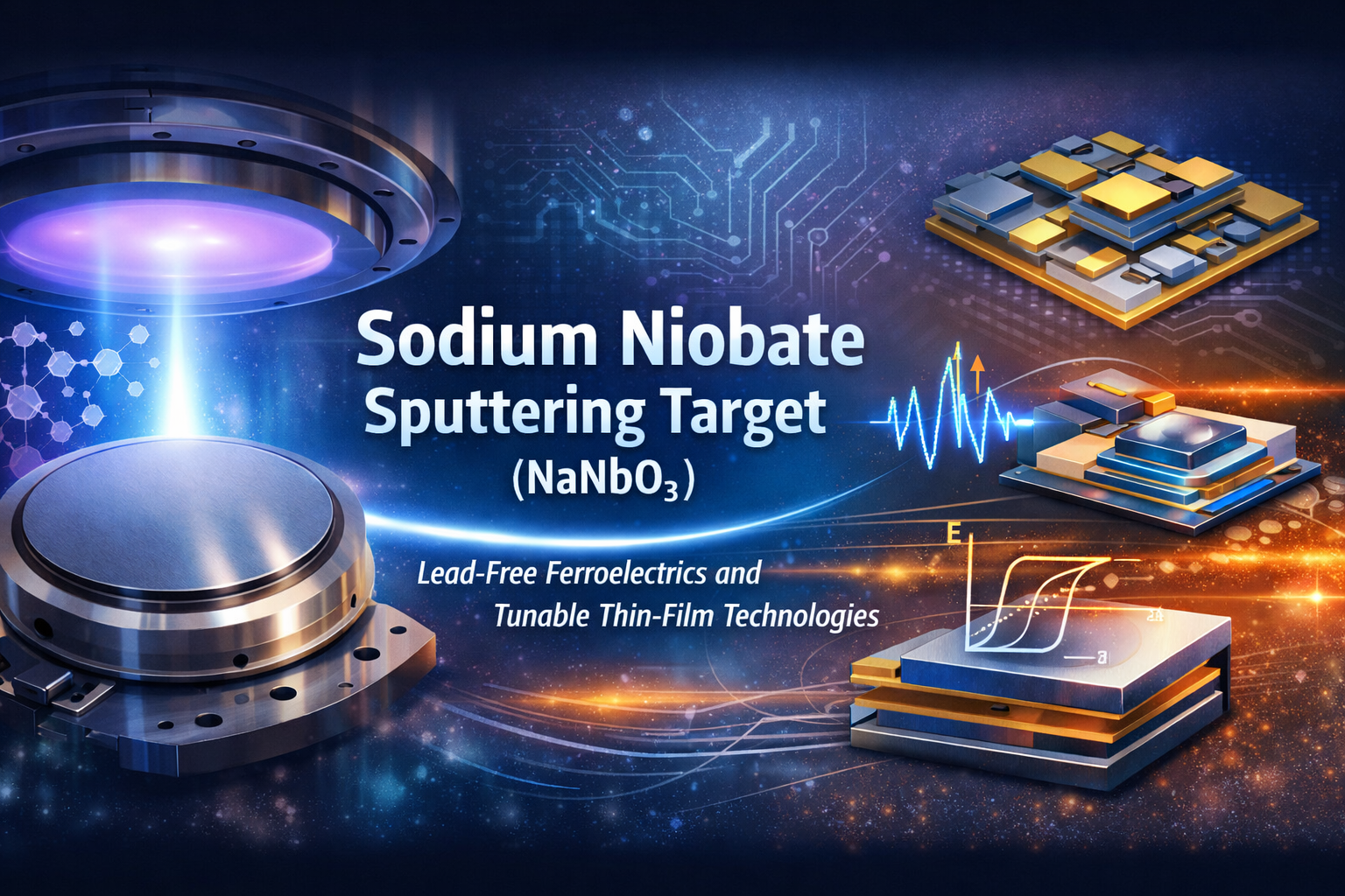
Introduction: Why Sodium Niobate Appears in Advanced Thin-Film Research
In the landscape of functional oxide thin films, Sodium Niobate (NaNbO₃) occupies a unique and often underestimated position. It is not a “mainstream” sputtering target like ZnO, Al₂O₃, or TiO₂, nor does it belong to the high-volume commercial ferroelectrics such as PZT. Instead, NaNbO₃ is typically selected intentionally and purpose-driven, when a project demands lead-free ferroelectric behavior, antiferroelectric characteristics, strong electromechanical coupling, or tunable dielectric properties under carefully controlled conditions.
As environmental regulations tighten and lead-free alternatives gain importance, Sodium Niobate thin films have drawn increasing attention in academic research, advanced sensor development, tunable RF devices, and emerging energy-related applications. In these contexts, sputtering targets of NaNbO₃ play a critical role by enabling precise compositional control, scalable deposition, and compatibility with modern PVD processes.
This article explains when Sodium Niobate sputtering targets are needed, what problems they solve, and which application scenarios justify their selection, providing a practical decision framework for engineers and researchers working in thin-film technologies.
Understanding Sodium Niobate as a Functional Oxide Material
Crystal Structure and Phase Behavior
Sodium Niobate (NaNbO₃) is a perovskite-structured oxide with rich phase transitions across temperature and electric field conditions. Unlike simple cubic oxides, NaNbO₃ exhibits:
- Antiferroelectric phases at room temperature
- Field-induced ferroelectric transitions
- Strong coupling between lattice distortion and polarization behavior
This complex phase behavior is not a drawback; rather, it is the primary reason NaNbO₃ is attractive in tunable and adaptive device architectures.
Why Sodium Matters in Thin Films
In oxide thin films, alkali elements such as sodium are notoriously challenging due to:
- High vapor pressure
- Potential sodium loss during deposition
- Sensitivity to oxygen partial pressure
However, when properly controlled, sodium incorporation enables distinct dielectric and polarization responses that cannot be replicated with alkaline-earth-based perovskites. This makes NaNbO₃ especially valuable in research-grade and niche industrial thin films, where performance outweighs processing simplicity.
When Do You Actually Need a Sodium Niobate Sputtering Target?
1. When Lead-Free Ferroelectric or Antiferroelectric Behavior Is Required
One of the most compelling reasons to use a NaNbO₃ sputtering target is the demand for lead-free ferroelectric or antiferroelectric materials.
Traditional ferroelectrics like Pb(Zr,Ti)O₃ (PZT) offer excellent performance but face increasing regulatory pressure due to lead content. Sodium Niobate provides:
- Zero lead content
- Stable perovskite structure
- Comparable dielectric tunability in certain regimes
For research groups developing RoHS-compliant devices or future-proof materials platforms, NaNbO₃ thin films represent a strategic alternative.
2. When Antiferroelectric Switching Is Beneficial

Unlike classic ferroelectrics, NaNbO₃ naturally stabilizes in an antiferroelectric phase, which allows:
- Double hysteresis loops
- Field-induced polarization switching
- Energy storage through phase transition
This makes Sodium Niobate sputtered films particularly relevant in:
- Pulsed power capacitors
- Energy storage research
- Adaptive dielectric systems
In such cases, NaNbO₃ is not a substitute material—it is a functional necessity.
3. When High Dielectric Tunability Is Needed Without High Loss
Sodium Niobate exhibits electric-field-dependent dielectric permittivity, making it suitable for tunable microwave and RF components, such as:
- Tunable capacitors
- Phase shifters
- Frequency-agile resonators
Compared to some ferroelectric oxides, NaNbO₃ can offer lower dielectric loss at moderate tunability, especially when thin-film microstructure and stoichiometry are well controlled via sputtering.
4. When Thin-Film Integration Is Required (Instead of Bulk Ceramics)
Many sodium niobate applications originate in bulk ceramics, but modern device integration increasingly demands thin-film formats:
MEMS-based actuators
On-chip sensors
Integrated RF components
Sputtering targets enable:
Thickness control down to tens of nanometers
Uniform deposition over wafers
Compatibility with silicon, sapphire, and oxide substrates
If a project requires device-scale integration, bulk NaNbO₃ ceramics are no longer sufficient—a sputtering target becomes essential.
Why Choose Sputtering for Sodium Niobate Thin Films?
Advantages Over Other Deposition Methods
While Chemical Solution Deposition (CSD) and PLD are sometimes used for NaNbO₃, magnetron sputtering offers several advantages:
- Better scalability
- Higher reproducibility
- Compatibility with industrial vacuum systems
- Cleaner film–substrate interfaces
For pilot production or multi-sample research programs, sputtering provides process stability that solution-based methods struggle to match.
Stoichiometry Control Challenges—and How Targets Solve Them
Sodium volatility is a known challenge. High-quality NaNbO₃ sputtering targets are engineered to:
- Compensate for sodium loss during deposition
- Maintain uniform Na/Nb ratio across the target
- Minimize compositional drift over target lifetime
This is where target density, phase purity, and fabrication method become critical, especially for reproducible thin-film research.
Key Application Scenarios for Sodium Niobate Sputtering Targets
1. Lead-Free Ferroelectric Thin-Film Research
Universities and research institutes frequently use NaNbO₃ sputtering targets in studies focused on:
- Polarization switching mechanisms
- Phase transition engineering
- Strain-induced property tuning
Such research often explores substrate-induced strain, oxygen stoichiometry, and dopant effects—areas where sputtered thin films outperform bulk samples.
2. Energy Storage and Antiferroelectric Capacitors
NaNbO₃ thin films are investigated for:
- High energy density capacitors
- Fast charge–discharge systems
- Pulse power electronics
The antiferroelectric-to-ferroelectric transition allows energy to be stored mechanically within the lattice, offering a different storage mechanism than conventional dielectrics.
3. Piezoelectric and Electromechanical Devices
Although not as widely commercialized as PZT, Sodium Niobate thin films are explored for:
- Micro-actuators
- Sensors in harsh environments
- MEMS components requiring lead-free materials
In these systems, film orientation and crystallinity, enabled by sputtering, are decisive factors.
4. Tunable RF and Microwave Components
NaNbO₃ thin films are studied for:
- Tunable dielectric layers
- RF capacitors
- Frequency-selective surfaces
The ability to tune dielectric constant with applied electric field makes NaNbO₃ attractive in reconfigurable RF systems, especially when environmental compliance is required.
5. Multiferroic and Heterostructure Research
Sodium Niobate is frequently combined with:
- Magnetic oxides
- Conductive perovskites
- Buffer layers for lattice matching
Sputtering targets allow layer-by-layer heterostructure fabrication, supporting research into coupled electric, magnetic, and mechanical phenomena.
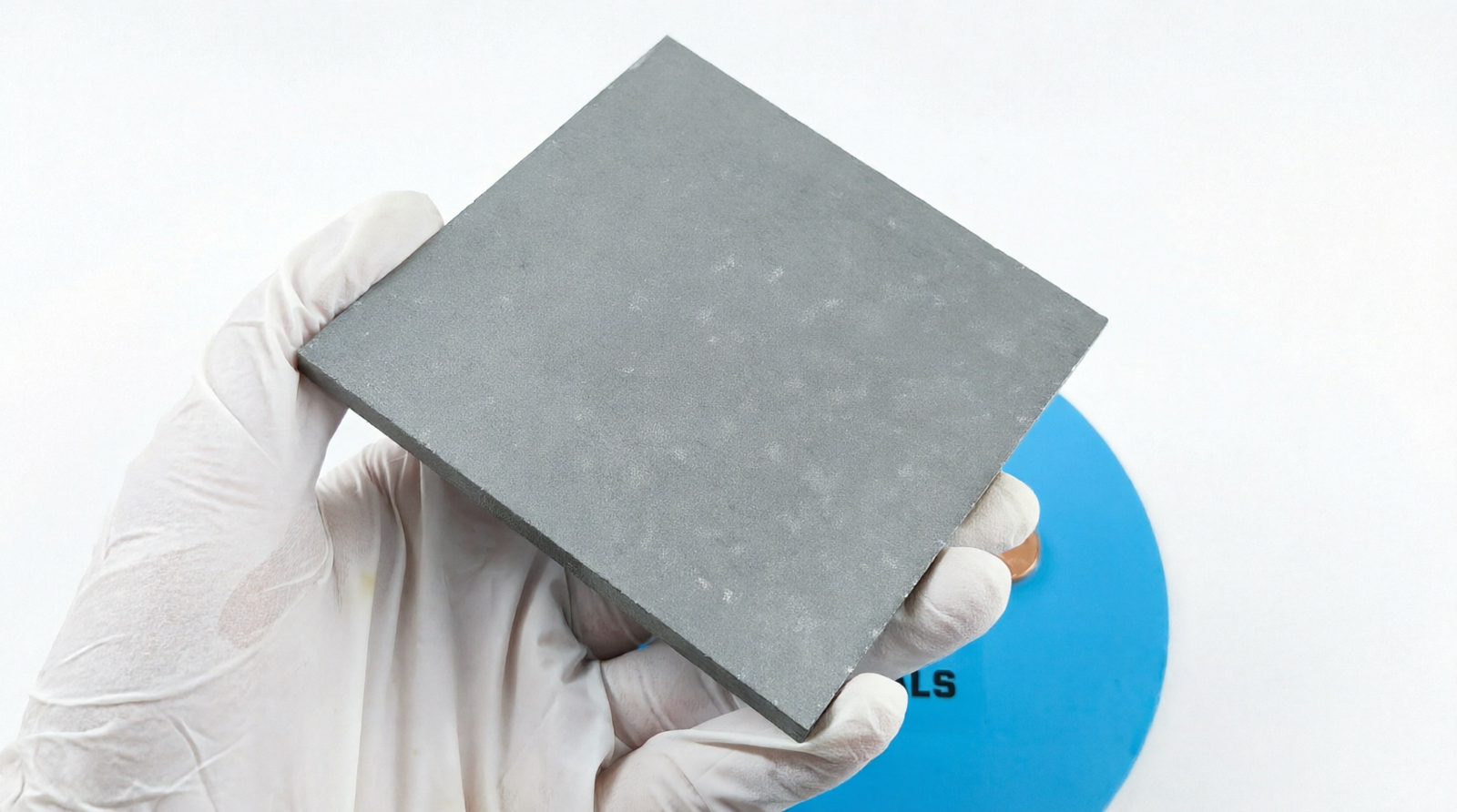
Typical Technical Parameters of NaNbO₃ Sputtering Targets
| Parameter | Typical Value / Range | Importance |
|---|---|---|
| Chemical Formula | NaNbO₃ | Defines perovskite functionality |
| Purity | 99.9% – 99.99% | Impacts dielectric loss and stability |
| Density | ≥95% theoretical | Ensures stable sputtering behavior |
| Diameter | 25 – 300 mm (custom) | Compatible with lab & production tools |
| Thickness | 3 – 6 mm | Influences target lifetime |
| Bonding | Indium / elastomer / Cu backing | Improves thermal management |
Processing Considerations: What Engineers Should Watch For
Sodium Volatility Management
- Lower sputtering power
- Optimized oxygen partial pressure
- Substrate temperature control
These factors are often more critical for NaNbO₃ than for transition-metal oxides.
Film Crystallization Strategy
Depending on application, films may be:
- Deposited amorphous and post-annealed
- Grown directly in a crystalline state
Target quality directly affects the feasibility of both approaches.
Why Target Quality Matters More for Sodium Niobate Than Many Oxides
NaNbO₃ is less forgiving than simple oxides. Inconsistent target composition can lead to:
- Sodium-deficient films
- Secondary phase formation
- Unstable electrical properties
For this reason, Sodium Niobate sputtering targets are typically sourced for high-value, low-volume applications, where performance consistency outweighs cost.
Packaging
Our Sodium Niobate Sputtering Targets (NaNbO₃) are meticulously tagged and labeled externally to ensure efficient identification and strict quality control. Each target is carefully packaged using protective cushioning and moisture-resistant materials to prevent contamination or mechanical damage during storage and transportation. These measures ensure the targets arrive in optimal condition for high-precision thin-film deposition.
Conclusion: When Sodium Niobate Is the Right Choice
A Sodium Niobate sputtering target is not selected casually—it is chosen when a project requires:
- Lead-free ferroelectric or antiferroelectric behavior
- Tunable dielectric properties
- Advanced thin-film integration
- Research-grade control over phase and composition
In these scenarios, NaNbO₃ is not just an alternative material; it is often the enabling material.
With proper target design, controlled sputtering conditions, and thoughtful device integration, Sodium Niobate thin films continue to play an important role in the future of functional oxides, environmentally compliant electronics, and advanced thin-film research.
For detailed specifications, customization options, and quotations, please contact sales@thinfilmmaterials.com.