Generic selectors
Exact matches only
Search in title
Search in content
Post Type Selectors

Thermal Oxide Silicon Wafers (Si+SiO2)

TFM Thermal Oxide Silicon Wafer – Your Trusted SiO₂ Wafer Provider

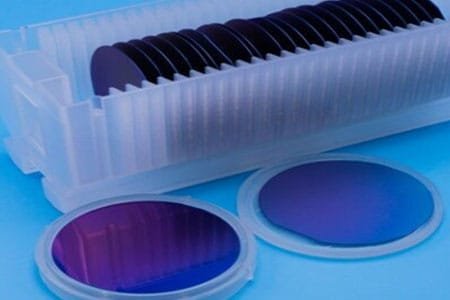
TFM offers high-quality Thermal Oxide Silicon Wafers (Si+SiO2), widely used in semiconductor, MEMS, and optoelectronic applications. These wafers consist of a silicon (Si) base layer with a precisely grown silicon dioxide (SiO₂) layer, providing superior electrical insulation, surface passivation, and enhanced device reliability.

Manufactured through a controlled thermal oxidation process, the SiO₂ layer ensures excellent uniformity, dielectric strength, and minimal defect density. These wafers are available in various oxide thicknesses, making them ideal for use in MOSFET fabrication, microfluidics, and optical coatings. Their high thermal and chemical stability allows for reliable performance in demanding environments.

TFM supplies customized Thermal Oxide Silicon Wafers tailored to meet the stringent requirements of research, industrial production, and advanced semiconductor development.

Thermal Oxide Silicon Wafer Specifications

Size10×10, 15×15, 20×15, 20×20 (customized sizes available) <br> Dia 1″, Dia 2″, Dia 3″, Dia 4″, Dia 5″, Dia 6″, Dia 8″, Dia 12″
Thickness0.3-0.5mm, 1.0mm
PolishedSSP or DSP
Orientation<100>, <110>, <111>
Redirection Precision±0.5°
Redirection the Edge2° (special in 1°)

Thermal Oxide Silicon Wafer Physical Properties

MaterialSi+SiO₂
StructureM3
Melting Point1420°C
Density (g/cm³)2.4 g/cm³
Doped MaterialsUndoped, B-doped, P-doped
TypeP / N, P, N
Resistivity>1000 Ωcm, 10⁻³ 40 Ωcm, 0.050.1 Ωcm
Thermal Expansion≤100/cm²
Oxide Thickness300~500nm (customized sizes available)

Reviews

There are no reviews yet.

Be the first to review “Thermal Oxide Silicon Wafers (Si+SiO2)”

Your email address will not be published. Required fields are marked *

FAQ

A thin film substrate is the base material upon which thin layers of materials are deposited to create electronic, optical, or mechanical devices. The substrate provides structural support and can influence the properties of the thin film.

The choice of substrate affects the film’s structural integrity, electrical properties, and overall performance. Factors like thermal expansion coefficient, surface smoothness, and chemical compatibility are crucial considerations.

Materials such as lanthanum aluminate (LaAlO₃), magnesium oxide (MgO), and strontium titanate (SrTiO₃) are commonly used due to their lattice compatibility and thermal stability, which are essential for optimal superconducting properties.

Metal substrates offer high electrical and thermal conductivity, making them suitable for applications requiring efficient heat dissipation and electrical connectivity. However, their surface properties and potential for oxidation must be managed during deposition.

These substrates are materials that can support the growth of thin films exhibiting magnetic or ferroelectric properties, essential for applications in memory devices, sensors, and actuators.

Semiconductor substrates, such as silicon wafers, serve as the foundation for integrated circuits and various electronic components, providing the necessary electrical characteristics and structural support for device fabrication.

Gallium Nitride (GaN) substrates are pivotal for high-performance optoelectronic and power devices due to their excellent thermal conductivity, high breakdown voltage, and efficiency. They are widely used in LEDs, power transistors, and RF components.

Halide crystal substrates, composed of halide compounds, are utilized in specialized optical applications, including infrared spectroscopy and laser systems, due to their unique optical properties.
Ceramic substrates provide high thermal stability, mechanical strength, and electrical insulation, making them ideal for high-frequency and high-power applications.
Proper surface preparation, including cleaning and polishing, ensures the removal of contaminants and surface irregularities, leading to improved film adhesion, uniformity, and performance.
Yes, thin films can be deposited on flexible substrates like polymers, enabling the development of flexible electronics and wearable devices. However, challenges include managing mechanical stress and ensuring film adhesion.
Challenges include ensuring lattice matching to minimize defects, managing thermal expansion differences to prevent stress and delamination, and achieving desired electrical and optical properties for specific applications.
Shopping Cart
Scroll to Top