1. Introduction
In recent decades, metal oxide semiconductors have been central to the advancement of thin film electronics. While n-type oxides such as ZnO, In₂O₃, and SnO₂ are well-established, the development of p-type oxide semiconductors has been limited by challenges in material stability and carrier mobility. Tin(II) oxide (SnO) has emerged as a rare exception: a p-type oxide semiconductor with a direct bandgap, high absorption coefficient, and potential for integration into thin film devices.
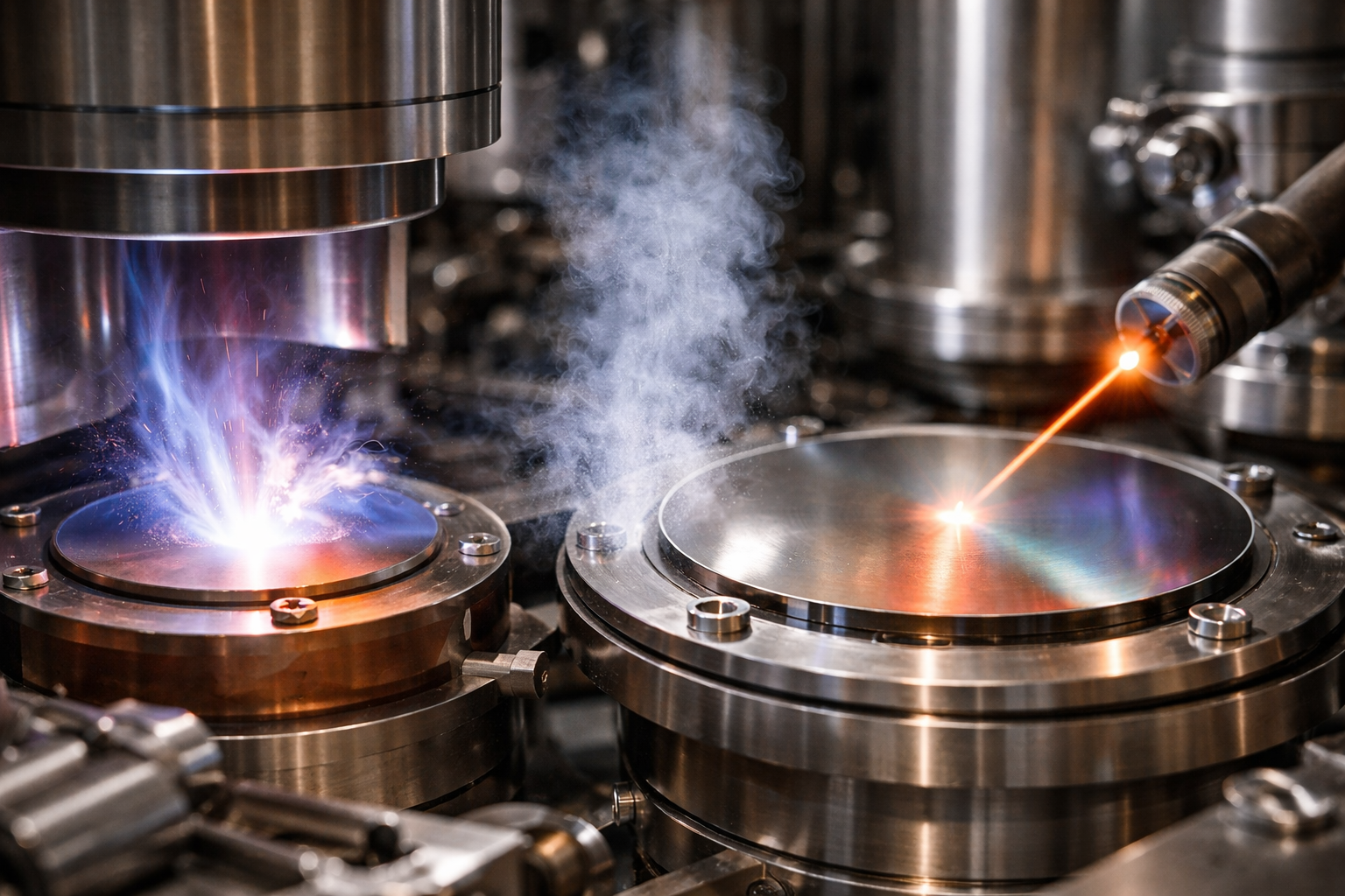
SnO sputtering targets are the source materials used in physical vapor deposition (PVD), particularly magnetron sputtering, to produce uniform and controlled SnO thin films. The metastable nature of SnO poses unique challenges during target preparation and sputtering, but its tunable properties make it an exciting material for transparent electronics, thin film solar cells, and novel optoelectronic devices.
This article explores the fundamentals of SnO sputtering targets, including their structural and electronic properties, manufacturing methods, film deposition mechanisms, and applications. The review also highlights ongoing research trends and the challenges of stabilizing SnO thin films for scalable industrial use.
2. Fundamentals of Tin(II) Oxide (SnO)
2.1 Crystal Structure
SnO crystallizes in a litharge-type tetragonal structure, where tin atoms are coordinated in a distorted square pyramidal environment with oxygen. Unlike SnO₂ (rutile structure), SnO is less thermodynamically stable and tends to oxidize to SnO₂, which complicates film deposition and long-term stability.
Key parameters:
- Crystal system: Tetragonal
- Lattice constants: a ≈ 3.80 Å, c ≈ 4.83 Å
- Density: ~6.45 g/cm³
2.2 Electronic Properties
SnO is a p-type semiconductor, with conductivity originating from tin vacancies that act as acceptor states. It features a:
- Direct bandgap: ~2.5–2.7 eV (suitable for optoelectronic absorption)
- Indirect bandgap: ~0.7 eV (enabling infrared absorption)
This dual bandgap behavior is of particular interest for all-oxide photovoltaic devices, where SnO can function as a light absorber.
2.3 Optical Characteristics
SnO thin films display moderate transparency in the visible spectrum while maintaining strong absorption in the near-infrared. This makes them suitable for tandem solar cells and selective optical coatings.
2.4 Comparison with SnO₂ and Sn₃O₄
- SnO₂: Stable n-type semiconductor, widely used as a transparent conductive oxide.
- Sn₃O₄: Mixed-valence oxide with intermediate properties.
- SnO: Metastable p-type semiconductor, offering unique opportunities for complementary oxide electronics when paired with n-type oxides.
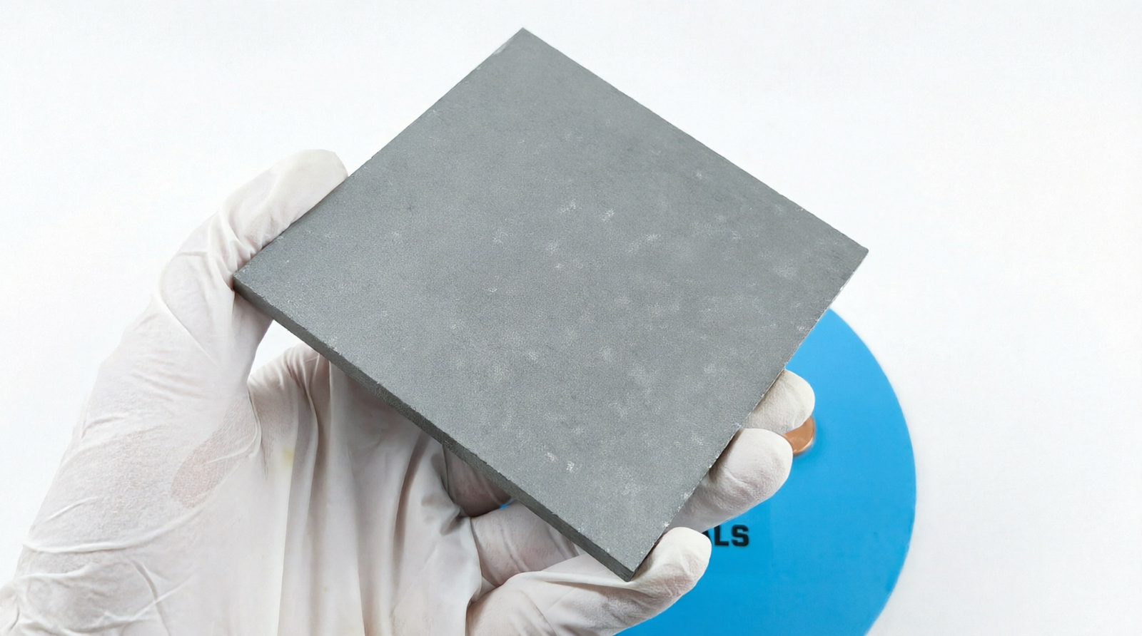
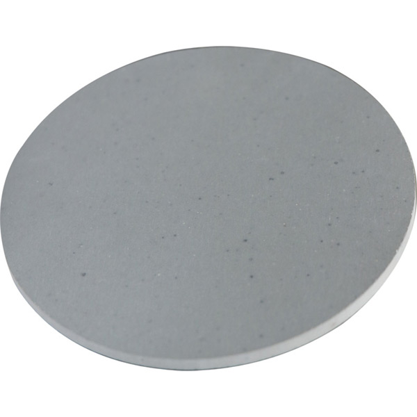
3. SnO Sputtering Target Fabrication
Producing high-quality SnO sputtering targets is challenging due to the metastable nature of SnO. Careful processing is required to prevent oxidation to SnO₂.
3.1 Raw Material Selection
- High-purity SnO powders (≥99.9%) are synthesized under controlled reducing atmospheres to maintain Sn²⁺ valence.
- Oxygen content must be carefully regulated to avoid over-oxidation.
3.2 Target Manufacturing Techniques
- Cold Isostatic Pressing (CIP) + Sintering: SnO powder is pressed into a compact form and sintered at moderate temperatures in inert or reducing atmospheres.
- Hot Pressing: Improves density but risks partial conversion to SnO₂ if oxygen control is inadequate.
- Spark Plasma Sintering (SPS): Provides rapid densification while minimizing oxidation, making it promising for high-purity SnO targets.
3.3 Target Characteristics
- Density: ≥90% theoretical density preferred for stable sputtering.
- Microstructure: Fine-grained targets improve sputtering stability.
- Bonding: Backing plates (copper or molybdenum) are often used to improve thermal conductivity and mechanical strength.
4. Stability Challenges in SnO Targets
SnO is thermodynamically metastable and tends to disproportionate into Sn and SnO₂ above ~300 °C. This instability poses challenges:
- Target cracking or degradation under high sputtering power.
- Non-stoichiometric films due to partial oxidation.
- Limited target lifespan compared with ZnO or SnO₂.
Mitigation strategies include:
- Processing in controlled atmospheres.
- Surface passivation of targets.
- Lower sputtering power densities to minimize thermal load.
5. Sputtering of SnO Thin Films
The deposition of SnO thin films via sputtering is complicated by the metastable nature of SnO, which readily converts to SnO₂ during processing. Nevertheless, magnetron sputtering of SnO targets under carefully controlled conditions has proven effective in producing functional p-type oxide films.
5.1 Magnetron Sputtering Configurations
- RF Magnetron Sputtering: Commonly used due to the semiconducting/insulating nature of SnO. RF fields prevent charge buildup on the target surface and yield stable plasma.
- DC Magnetron Sputtering: Possible if the target conductivity is sufficiently high, but usually avoided due to arcing issues.
- Pulsed DC Sputtering: Can improve plasma stability while minimizing arcing compared with conventional DC.
5.2 Process Parameters
Achieving stoichiometric SnO films requires fine-tuning several parameters:
- Working gas composition: Argon (Ar) with a controlled partial pressure of oxygen (O₂). Too much oxygen causes oxidation to SnO₂, while too little promotes metallic Sn.
- Substrate temperature: Elevated substrate temperatures (~100–300 °C) improve crystallinity but risk SnO disproportionation. Low-temperature sputtering followed by controlled annealing is often employed.
- Power density: Excessive power can overheat targets, triggering SnO decomposition. Moderate power densities are preferred.
- Chamber pressure: Affects plasma stability and film density. Pressures between 1–10 mTorr are typical.
5.3 Reactive Sputtering Approach
In some cases, metallic Sn targets are sputtered in an oxygen-containing atmosphere to form SnO films. However, this is extremely challenging:
- Oxygen flow must be precisely balanced to avoid forming SnO₂ instead of SnO.
- Target poisoning (insulating oxide layer formation) complicates process stability.
For this reason, direct SnO ceramic targets are generally preferred over reactive sputtering.
6. Thin Film Characteristics
6.1 Structural Properties
Sputtered SnO films often crystallize in the litharge structure, with strong orientation along the (001) or (101) planes. However, maintaining single-phase SnO is challenging: secondary phases such as Sn or SnO₂ often coexist, depending on deposition conditions.
- Single-phase SnO: Achieved under optimized oxygen partial pressure and low substrate temperatures.
- Mixed phases: May exhibit altered optical/electronic properties but often degrade p-type conductivity.
6.2 Electrical Properties
- Conductivity type: SnO is intrinsically p-type, due to tin vacancies acting as acceptors.
- Carrier concentration: Typically 10¹⁵–10¹⁷ cm⁻³, lower than n-type oxides like ZnO.
- Mobility: ~1–10 cm²/V·s, which is modest compared with conventional semiconductors but sufficient for thin film devices.
The difficulty lies in maintaining stable p-type conduction, as unintentional oxidation or defect compensation often suppresses hole mobility.
6.3 Optical Properties
SnO films exhibit unique dual bandgap absorption:
- Indirect bandgap (~0.7 eV): Enables near-infrared absorption.
- Direct bandgap (~2.5–2.7 eV): Provides visible light absorption.
This makes SnO attractive for broad-spectrum photovoltaics and tandem solar cell structures. Optical transparency is typically 70–85% in the visible range, depending on thickness and phase purity.
6.4 Surface Morphology
AFM and SEM studies of sputtered SnO films reveal:
- Fine-grained, smooth films under optimized conditions.
- Rougher, porous films at high oxygen pressures.
- Columnar microstructures in thicker films.
Surface morphology strongly affects gas-sensing performance and interface quality in heterojunction devices.
7. Post-Deposition Treatments
Post-processing is often required to stabilize and enhance SnO films.
- Annealing: Performed in reducing atmospheres (Ar, N₂, forming gas) at moderate temperatures (<300 °C). Enhances crystallinity and carrier concentration. Excessive annealing risks SnO disproportionation.
- Plasma Treatments: Oxygen or hydrogen plasma can tune surface states and carrier density.
- Laser Annealing: Provides localized heating to improve crystallinity without subjecting the whole substrate to high temperatures.
8. Doping and Defect Engineering
The inherent limitation of SnO is its low hole mobility and instability. Researchers are investigating doping strategies to enhance performance:
- Alkali Metals (Na, K): Introduced into SnO films to increase hole concentration.
- Group V Elements (N, P): Nitrogen doping is explored for stabilizing p-type conduction, though incorporation is difficult.
- Alloying with Other Oxides: SnO-SnO₂ mixed phases can yield ambipolar behavior, while SnO-ZnO alloys may improve band alignment for photovoltaics.
Defect engineering, particularly controlling oxygen vacancies and tin interstitials, is equally important for achieving reproducible electronic behavior.
9. Applications of SnO Thin Films
9.1 Photovoltaics
SnO has emerged as a promising candidate for next-generation solar cells due to its p-type conductivity and suitable band alignment.
- Heterojunction Solar Cells: SnO films serve as hole-transport layers in tandem solar cells. When paired with n-type semiconductors like ZnO or SnO₂, they form efficient p–n junctions.
- Perovskite Solar Cells: SnO can function as a hole extraction layer in perovskite architectures, improving stability and reducing recombination.
- All-Oxide Solar Cells: Efforts are underway to create fully oxide-based photovoltaics (SnO as the p-type absorber and ZnO as the n-type partner), offering low-cost, stable alternatives to silicon.
The key challenge is maintaining pure-phase SnO with high hole mobility during deposition and operation.
9.2 Thin-Film Transistors (TFTs)
In display technologies, SnO offers potential as a p-type channel material in TFTs. While n-type oxide semiconductors (like IGZO and ZnO) are widely used, the lack of reliable p-type oxides limits complementary circuits.
- Complementary Circuits: Incorporating SnO TFTs with n-type oxides enables CMOS-like designs, reducing power consumption.
- Stability: Although SnO TFTs exhibit modest performance (μ ≈ 1 cm²/V·s, Ion/Ioff ≈ 10⁴), research shows improved device uniformity through optimized sputtering.
- Flexible Electronics: SnO TFTs deposited at low temperatures (<200 °C) are compatible with plastic substrates, making them suitable for flexible displays and wearables.
9.3 Gas Sensors
SnO thin films demonstrate sensitivity to reducing gases (H₂, CO, CH₄) and certain oxidizing gases (O₂, NO₂).
- Mechanism: Adsorption of gas molecules alters surface carrier concentration, leading to measurable resistance changes.
- Selectivity: SnO sensors show enhanced selectivity toward CO compared with SnO₂, due to their different surface chemistry.
- Operating Temperature: SnO sensors often function at lower operating temperatures (150–250 °C), reducing power consumption compared with traditional SnO₂ sensors (>300 °C).
9.4 Memory Devices
SnO-based thin films are being explored for resistive random-access memory (ReRAM).
- Mechanism: Resistive switching occurs through oxygen vacancy migration, altering the conductive state.
- Advantage: SnO films offer tunable band alignment and compatibility with CMOS processes.
- Challenge: Phase instability during high-field operation remains an obstacle.
9.5 Protective and Optical Coatings
Due to their transparency and hardness, SnO coatings find use in protective films for displays and optical elements.
- Anti-Reflective Films: SnO can reduce reflection losses in optical devices.
- Wear-Resistant Layers: Its chemical resistance enhances durability in industrial glass and sensor applications.
- UV Protection: SnO films exhibit strong UV absorption, useful for display and photovoltaic encapsulation.
10. Industrial and Commercial Relevance
10.1 Market Demand
The commercial use of SnO sputtering targets remains limited compared with ZnO and SnO₂. However, interest is rising due to the need for reliable p-type oxides. Key drivers include:
- Growth of tandem photovoltaics requiring optimized hole transport layers.
- Development of transparent electronics and flexible displays.
- Rising demand for oxide-based semiconductors in energy-efficient devices.
10.2 Fabrication Challenges
- Target Fragility: SnO targets are mechanically weaker than metallic Sn or SnO₂, requiring careful handling.
- Stoichiometry Control: Maintaining pure Sn²⁺ during sintering and deposition is difficult.
- Phase Purity: Avoiding SnO₂ contamination is essential for reproducible device performance.
10.3 Commercial Suppliers
Several advanced materials companies are beginning to offer SnO sputtering targets in research-grade purities (≥99.9%). They are typically supplied as:
- Ceramic targets: Produced via hot pressing or sintering.
- Bonded targets: Backed with copper or molybdenum plates to improve thermal conductivity and prevent cracking.
As demand for oxide-based p–n junctions grows, supply chains for SnO targets are expected to expand.
11. Comparative Analysis with Other Oxide Targets
| Parameter | SnO | SnO₂ | ZnO | IGZO |
|---|---|---|---|---|
| Conductivity Type | p-type | n-type | n-type (tunable) | n-type |
| Bandgap | Indirect 0.7 eV, Direct ~2.7 eV | ~3.6 eV | ~3.3 eV | ~3.0 eV |
| Transparency | High in visible | High in visible | High in visible | High in visible |
| Applications | p-type TFTs, photovoltaics, sensors | Transparent conductors (TCOs), gas sensors | Transparent conductors, LEDs, TFTs | Displays, flexible electronics |
| Challenges | Phase instability, low mobility | Limited p-type doping | Limited p-type doping | High indium cost |
This comparison highlights the unique niche of SnO as one of the few oxide semiconductors with intrinsic p-type behavior. While SnO₂ and ZnO dominate current industrial use, SnO’s role may grow as complementary oxide electronics and tandem solar cells mature.
12. Future Prospects
Research into SnO sputtering targets is rapidly evolving. Promising directions include:
- Stabilization Techniques: Developing composite SnO-based targets to reduce phase transitions.
- Doping Strategies: Enhancing hole mobility through alkali metal or nitrogen doping.
- Hybrid Architectures: Integrating SnO with perovskites or organic semiconductors for next-generation optoelectronics.
- Low-Temperature Deposition: Expanding applications in flexible substrates and wearable electronics.
In the long term, SnO could become a critical enabler for all-oxide semiconductor devices, particularly in photovoltaics and transparent electronics.