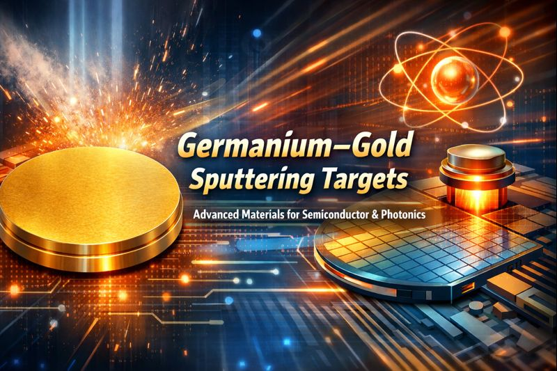
Introduction
In advanced thin-film deposition for semiconductor and electronic devices, material selection is rarely driven by a single property. Electrical performance, interfacial behavior, thermal stability, compatibility with downstream processes, and long-term reliability all play equally critical roles. Among the many alloy systems used in physical vapor deposition (PVD), Germanium–Gold (GeAu) sputtering targets have established a distinctive position, particularly in applications where controlled electrical contact behavior and stable metal–semiconductor interfaces are required.
Unlike pure metals or simple elemental targets, GeAu combines the intrinsic advantages of both germanium and gold into a tunable alloy system. This article provides a comprehensive analysis of why engineers and researchers choose Germanium–Gold sputtering targets, how they compare with alternative materials, and which application scenarios benefit most from their unique properties.
Understanding the Germanium–Gold Alloy System
Atomic-Level Design Philosophy
A typical Germanium–Gold sputtering target is specified by atomic percentage rather than weight percentage—for example, Ge 80 at.% / Au 20 at.%. This distinction is important because thin-film electrical and interfacial behavior are governed primarily by atomic distribution and bonding, not mass contribution.
At the atomic scale:
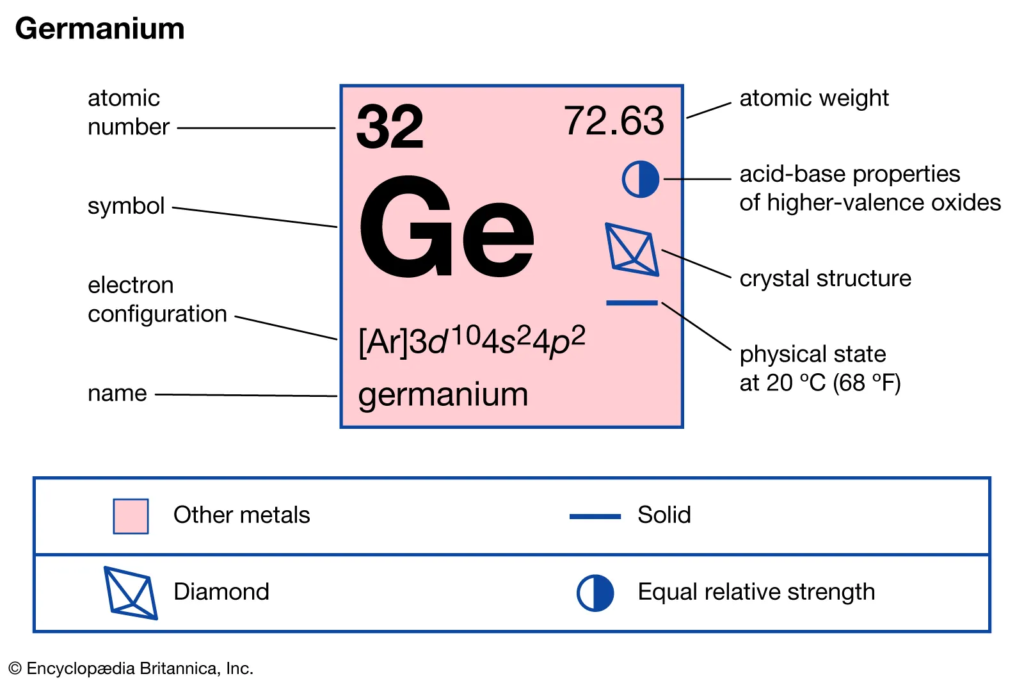
- Germanium (Ge) contributes semiconductor-like behavior, band structure compatibility, and controlled diffusion characteristics.
- Gold (Au) contributes high electrical conductivity, chemical inertness, and stable metallic bonding.
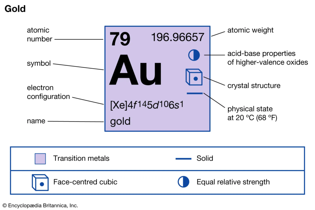
The resulting alloy film exhibits hybrid behavior, positioned between pure semiconductor films and noble-metal conductive layers.
Microstructural Stability
GeAu alloys form relatively stable microstructures during sputtering and post-deposition thermal treatment. Compared with pure Au films—which can agglomerate or dewet at elevated temperatures—GeAu films demonstrate:
- Improved grain boundary stability
- Reduced film discontinuity risk
- Better interface adhesion on semiconductor substrates
These characteristics are especially valuable in micro- and nano-scale device architectures.
Key Advantages of Germanium–Gold Sputtering Targets
1. Optimized Electrical Contact Performance
One of the primary reasons for selecting GeAu is its controlled electrical contact behavior.
- Pure gold offers excellent conductivity but can form unstable or high-resistance interfaces with certain semiconductors.
- Germanium introduces energy band alignment that helps reduce Schottky barrier height or enables near-ohmic contact formation in specific device structures.
As a result, GeAu films are widely used where predictable and reproducible contact resistance is critical.
2. Superior Metal–Semiconductor Interface Compatibility
ermanium has long been used in semiconductor technology due to its favorable electronic properties. When alloyed with gold:
Interfacial reactions become more controllable
Diffusion behavior can be tailored through composition
Adhesion to Ge-based or III–V semiconductor substrates improves
Compared with pure Au layers, GeAu films are less prone to delamination or uncontrolled interdiffusion during annealing.
3. Enhanced Thermal Stability Compared with Pure Gold
While gold is chemically stable, it is not always thermally stable in thin-film form. Pure Au films can:
- Recrystallize rapidly
- Agglomerate at moderate temperatures
- Lose continuity in fine features
The presence of germanium helps suppress these effects, providing:
- Improved thermal endurance
- Better film morphology retention
- Increased process window during thermal cycling
This makes GeAu particularly suitable for post-deposition annealing steps common in semiconductor manufacturing.
4. High Chemical Inertness with Functional Tunability
Gold’s noble nature ensures resistance to oxidation and corrosion. Germanium, while more reactive, is stabilized within the alloy matrix. Together, they offer:
- Long-term chemical stability
- Compatibility with vacuum, inert, and mildly reactive process environments
- Minimal contamination risk for sensitive devices
This balance is difficult to achieve with many alternative alloy systems.
5. Excellent Sputtering Behavior and Film Uniformity
From a process engineering perspective, GeAu sputtering targets offer:
- Stable sputtering rates
- Low particulate generation
- Uniform erosion profiles
- Good compositional transfer from target to film
These characteristics contribute to excellent thickness and composition uniformity, even on large-area substrates.
Comparison with Alternative Materials
GeAu vs. Pure Gold (Au) Targets
| Aspect | Pure Au | GeAu Alloy |
|---|---|---|
| Electrical Conductivity | Excellent | Very high (slightly reduced) |
| Interface Stability | Moderate | High |
| Thermal Stability | Limited | Improved |
| Adhesion to Semiconductors | Often requires adhesion layers | Intrinsically better |
| Process Flexibility | Limited | Broader |
Conclusion:
GeAu sacrifices a small amount of conductivity in exchange for much better interface control and thermal reliability.
GeAu vs. Pure Germanium (Ge) Targets
| Aspect | Pure Ge | GeAu Alloy |
|---|---|---|
| Conductivity | Moderate | High |
| Chemical Stability | Moderate | High |
| Contact Resistance | Higher | Lower |
| Film Robustness | Moderate | Improved |
Conclusion:
GeAu provides a conductive pathway without losing germanium’s favorable semiconductor interactions.
GeAu vs. Ti/Au or Cr/Au Multilayer Systems
Traditional metal stacks such as Ti/Au or Cr/Au are widely used but come with trade-offs:
- Additional deposition steps
- Interface complexity
- Potential diffusion between layers
GeAu offers a single-material solution that simplifies processing while delivering comparable or superior performance in many applications.
Major Application Scenarios
1. Semiconductor Ohmic and Quasi-Ohmic Contacts
GeAu is frequently selected for:
- Ge-based semiconductor devices
- III–V compound semiconductors
- Specialized contact layers requiring controlled barrier behavior
Its ability to balance conductivity and interface chemistry makes it ideal for precision contact engineering.
2. Infrared and Photodetector Devices
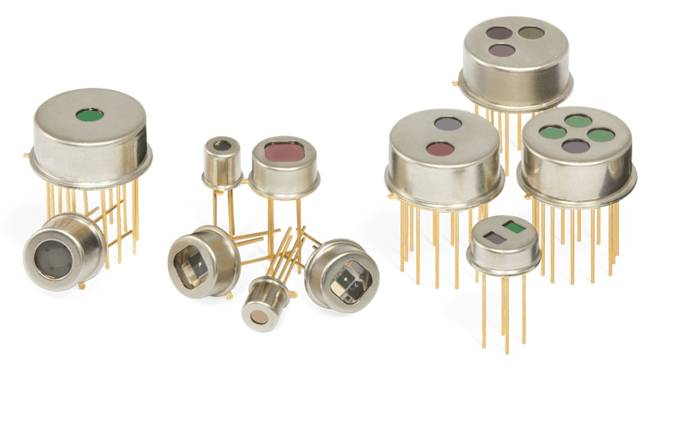
In IR detectors and photonic devices:
- Contact uniformity
- Low noise
- Thermal stability
are essential. GeAu films are commonly used as electrode or interconnect layers, especially in devices operating across temperature ranges.
3. Microelectronics and Advanced Packaging
In micro-scale interconnects and packaging structures, GeAu offers:
- Strong adhesion
- Reliable electrical pathways
- Resistance to long-term degradation
These properties support high-density integration and miniaturization trends.
4. MEMS and Sensor Technologies
MEMS devices often experience mechanical stress, thermal cycling, and environmental exposure. GeAu thin films provide:
- Mechanical robustness
- Stable electrical performance
- Good compatibility with silicon and compound substrates
This makes them suitable for sensors, actuators, and hybrid micro-systems.
5. Research and Development of Novel Thin Films
In academic and industrial R&D, GeAu sputtering targets are widely used for:
- Contact physics studies
- Interface engineering research
- Prototyping next-generation semiconductor devices
Their tunable composition allows researchers to explore structure–property relationships with high precision.
Manufacturing and Quality Considerations
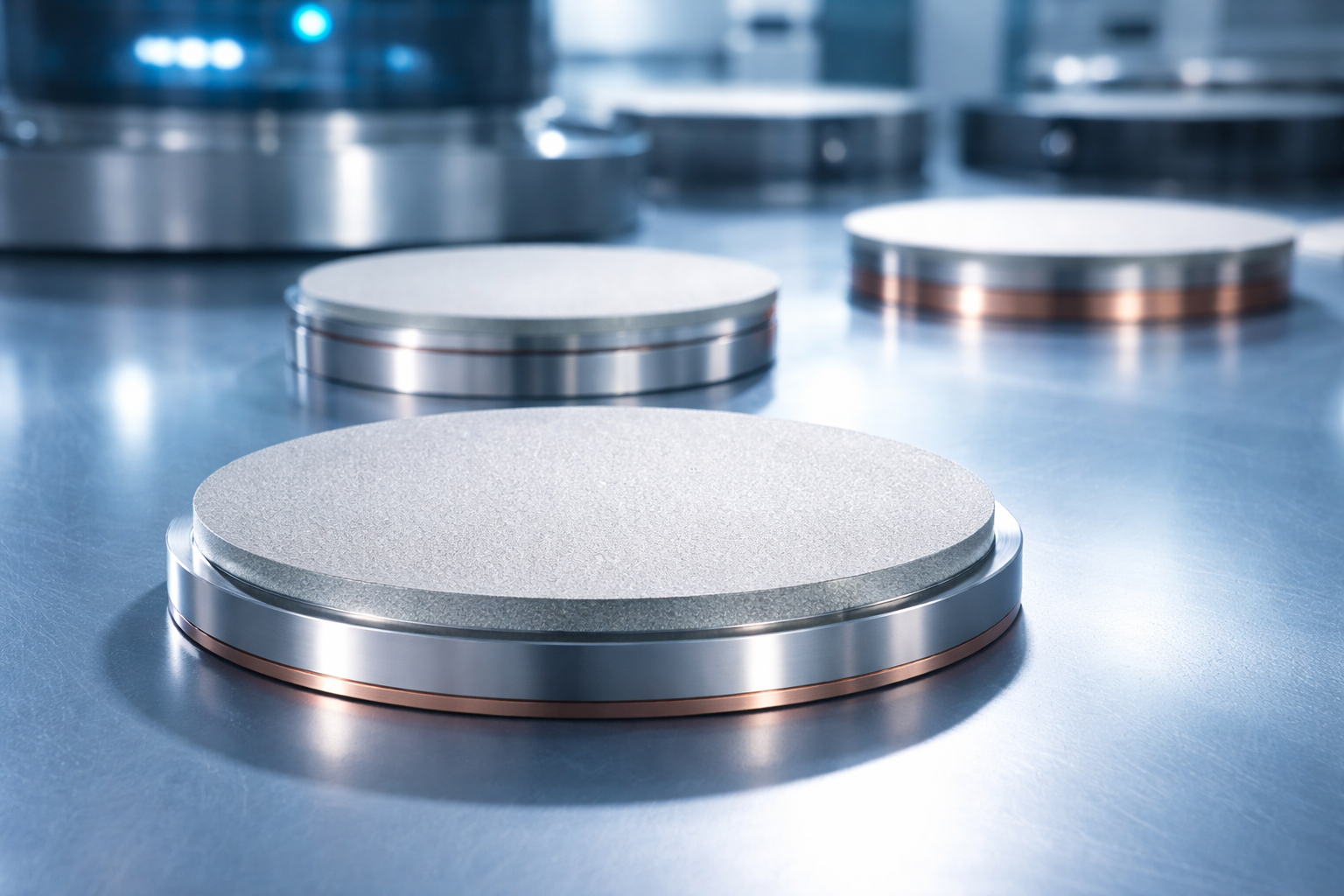
High-quality GeAu sputtering targets typically feature:
- High purity (commonly 99.99% or higher)
- Controlled alloy homogeneity
- Dense microstructure for stable sputtering
- Precise dimensional tolerances for standard cathodes
Proper target fabrication directly influences film quality, process repeatability, and system uptime.
Why Engineers Continue to Choose GeAu
The long-term adoption of Germanium–Gold sputtering targets is not accidental. It reflects a convergence of practical manufacturing needs and advanced device physics:
- Predictable performance
- Reduced process complexity
- Balanced electrical and interfacial properties
- Compatibility with existing PVD infrastructure
In many applications, GeAu is not merely an alternative—it is the most efficient engineering solution.
Conclusion
Germanium–Gold sputtering targets occupy a critical niche in thin-film deposition technologies. By combining the semiconductor compatibility of germanium with the conductivity and chemical stability of gold, GeAu delivers a uniquely balanced material system. Compared with pure metals or multilayer stacks, it offers superior interface control, enhanced thermal stability, and reliable electrical performance.
For semiconductor contacts, photonic devices, MEMS, and advanced research applications, GeAu continues to be a preferred choice where performance consistency and process reliability matter most.
For detailed specifications, composition options, and quotations for Germanium–Gold sputtering targets, please contact us at sales@thinfilmmaterials.com.