
 MSDS File
CIGS (CuInₓGa₁₋ₓSe₂) Pellet Evaporation Material
Introduction
CIGS (Copper Indium Gallium Selenide, CuInₓGa₁₋ₓSe₂) pellet evaporation material is a crucial compound source for thin film deposition, particularly in the fabrication of high-efficiency photovoltaic devices. By tuning the indium-to-gallium ratio (ₓ), researchers and manufacturers can optimize bandgap properties, enabling superior performance in solar cells, optoelectronic devices, and advanced coating applications.
Detailed Description
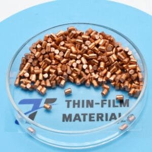
CIGS evaporation materials are engineered in the form of dense, uniform pellets, ensuring stable evaporation behavior under vacuum deposition conditions. Produced from high-purity precursors (≥99.9%), these pellets maintain consistent stoichiometry, which is essential for achieving reproducible thin film compositions.
Key features include:
Bandgap Tunability (1.0–1.7 eV) – adjustable by varying the In/Ga ratio, optimizing solar absorption efficiency.
High Purity – minimizes impurities and enhances thin film performance.
Pellet Form Factor – allows easy handling and stable evaporation in e-beam and thermal evaporation systems.
Uniform Stoichiometry – ensures reproducible deposition results across different production runs.
Versatility – suitable for both research and industrial-scale thin film solar cell manufacturing.
Applications
CIGS evaporation materials are widely used in:
Photovoltaics – thin film solar cell absorber layers.
Optoelectronics – devices requiring tunable bandgaps and high absorption coefficients.
R&D – semiconductor research in renewable energy and electronic materials.
Thin Film Coatings – functional coatings in energy and optical industries.
Pilot & Production Lines – scalable deposition processes for CIGS solar modules.
Technical Parameters
| Parameter | Typical Value / Range | Importance |
|---|---|---|
| Purity | 99.9% – 99.99% | Ensures minimal contamination |
| Composition | CuInₓGa₁₋ₓSe₂ (ₓ adjustable 0–1) | Bandgap control for solar efficiency |
| Form | Pellet | Stable for evaporation sources |
| Particle Size | 3 – 12 mm (customizable) | Matches crucible/e-beam needs |
| Bandgap Range | 1.0 – 1.7 eV | Optimized for photovoltaic applications |
Comparison with Related Materials
| Material | Key Advantage | Typical Application |
|---|---|---|
| CIGS (CuInₓGa₁₋ₓSe₂) | Tunable bandgap, high efficiency | Thin film solar cells |
| CIS (CuInSe₂) | Narrow bandgap (~1.0 eV) | Low-bandgap PV, R&D |
| CGS (CuGaSe₂) | Wider bandgap (~1.7 eV) | Tandem PV, optoelectronics |
FAQ
| Question | Answer |
|---|---|
| Can the In/Ga ratio be customized? | Yes, the composition can be tailored to achieve desired bandgaps. |
| What deposition methods are suitable? | Both e-beam evaporation and thermal evaporation are applicable. |
| Is this material used in commercial solar modules? | Yes, CIGS is one of the leading thin film absorber materials in industry. |
| How is it packaged? | Vacuum-sealed in moisture-protected containers, shipped in export-safe cartons or wooden crates. |
| What industries benefit most? | Photovoltaic manufacturing, optoelectronics, and semiconductor research. |
Packaging
Each batch of CIGS pellets is vacuum-sealed with protective inert gas to prevent oxidation. Packaging includes anti-static bags, foam cushioning, and export-grade cartons or wooden crates, ensuring safe delivery and long-term storage stability.
Conclusion
CIGS (CuInₓGa₁₋ₓSe₂) pellet evaporation material offers a tunable and high-efficiency solution for thin film solar cells and advanced optoelectronic applications. With high purity, stable pellet form, and customizable composition, it remains a leading choice for both research and industrial-scale production.
For detailed specifications and a quotation, please contact us at [sales@thinfilmmaterials.com].

Reviews
There are no reviews yet.