Introduction
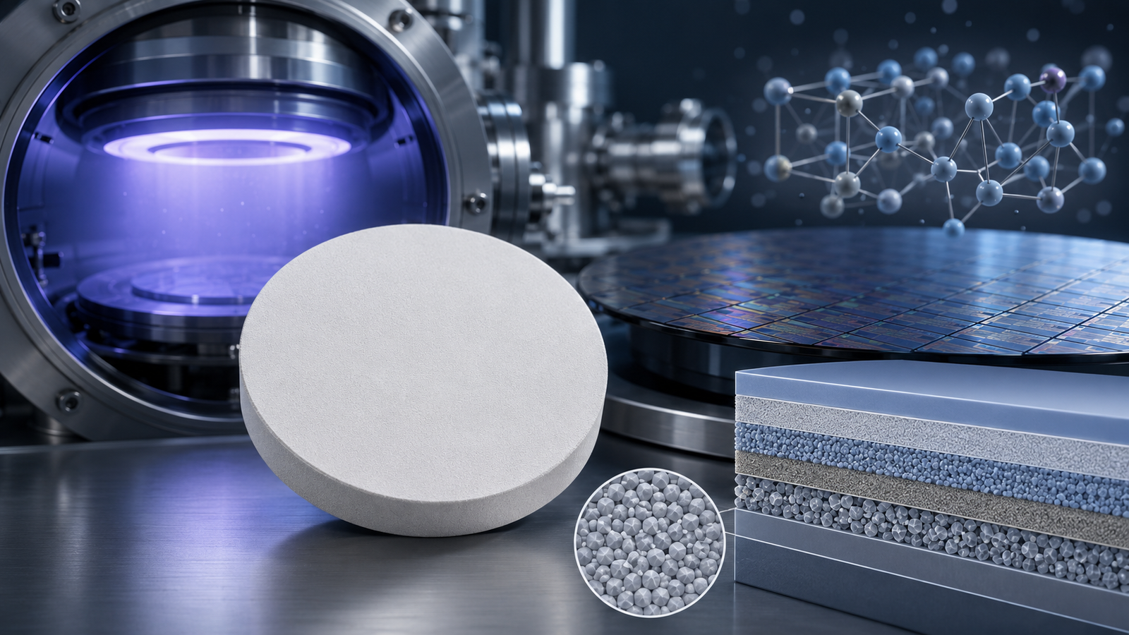
Titanium Silicate (Ti–Si–O) sputtering targets are gaining increasing attention in advanced thin film deposition due to their unique combination of dielectric stability, chemical durability, and tunable optical properties. As industries such as semiconductors, optics, and energy devices demand higher performance coatings, composite oxide targets like titanium silicate offer a versatile solution that bridges the gap between traditional silica-based and titanium oxide-based materials.
This article provides a comprehensive technical overview of titanium silicate sputtering targets, including their composition, deposition characteristics, and key applications in modern thin film technologies.
What Is Titanium Silicate?
Titanium silicate is a compound material composed primarily of titanium dioxide (TiO₂) and silicon dioxide (SiO₂) in varying ratios. Unlike pure oxide targets, titanium silicate belongs to a class of mixed oxide ceramics, where the combination of elements enables tailored film properties.
Depending on the stoichiometry and preparation method, titanium silicate can exist in amorphous or crystalline phases. The most commonly used compositions in sputtering targets are engineered to achieve:
- Improved dielectric strength
- Controlled refractive index
- Enhanced thermal stability
- Reduced film stress
This makes titanium silicate particularly suitable for precision thin film applications.
Why Use Titanium Silicate Sputtering Targets?
1. Tunable Optical Properties
By adjusting the Ti:Si ratio, titanium silicate films can achieve a wide range of refractive indices. Compared to pure SiO₂ (low index) and TiO₂ (high index), titanium silicate offers intermediate values, making it ideal for multilayer optical coatings.
2. Enhanced Chemical Stability
The incorporation of silicon improves resistance to corrosion and environmental degradation, which is critical for coatings exposed to harsh conditions.
3. Reduced Film Stress
Pure TiO₂ films often suffer from high intrinsic stress, which can lead to cracking or delamination. Adding SiO₂ helps mitigate this issue, resulting in more stable and adherent films.
4. Improved Process Compatibility
Titanium silicate targets are compatible with standard RF and DC magnetron sputtering systems, making them easy to integrate into existing deposition setups.
Deposition Behavior in Sputtering Processes
Titanium silicate targets are typically used in RF magnetron sputtering due to their insulating or semi-insulating nature. However, depending on composition and conductivity, some formulations may also support pulsed DC sputtering.
Key Deposition Characteristics
- Stable Plasma Formation: The mixed oxide composition helps maintain consistent plasma during sputtering.
- Low Particle Generation: High-density targets reduce arcing and particle contamination.
- Uniform Film Growth: Suitable for large-area coatings and high-uniformity requirements.
Process Parameters to Optimize
| Parameter | Typical Range | Impact |
|---|---|---|
| Power Density | 2–6 W/cm² | Controls deposition rate |
| Working Pressure | 1–10 mTorr | Affects film density |
| Substrate Temperature | Room temp – 400°C | Influences crystallinity |
| Gas Composition | Ar / Ar + O₂ | Controls stoichiometry |
Proper optimization of these parameters ensures high-quality films with consistent properties.
Applications of Titanium Silicate Thin Films
1. Optical Coatings
Titanium silicate is widely used in optical applications where precise refractive index control is required:
- Anti-reflective coatings
- Optical filters
- Waveguides
- Protective coatings for lenses
Its ability to fine-tune optical performance makes it a preferred material in multilayer designs.
2. Semiconductor Devices
In semiconductor manufacturing, titanium silicate films are used as dielectric layers due to their:
- High breakdown voltage
- Low leakage current
- Excellent thermal stability
Applications include:
- Gate dielectrics
- Interlayer dielectrics
- Passivation layers
3. Thin Film Transistors (TFTs)
Titanium silicate can serve as a gate insulator or buffer layer in TFT structures, particularly in display technologies such as:
- LCD panels
- OLED displays
- Flexible electronics
4. Energy and Functional Coatings
The material is also used in advanced energy systems:
- Protective coatings for photovoltaic devices
- Barrier layers in solid-state batteries
- Functional coatings for sensors
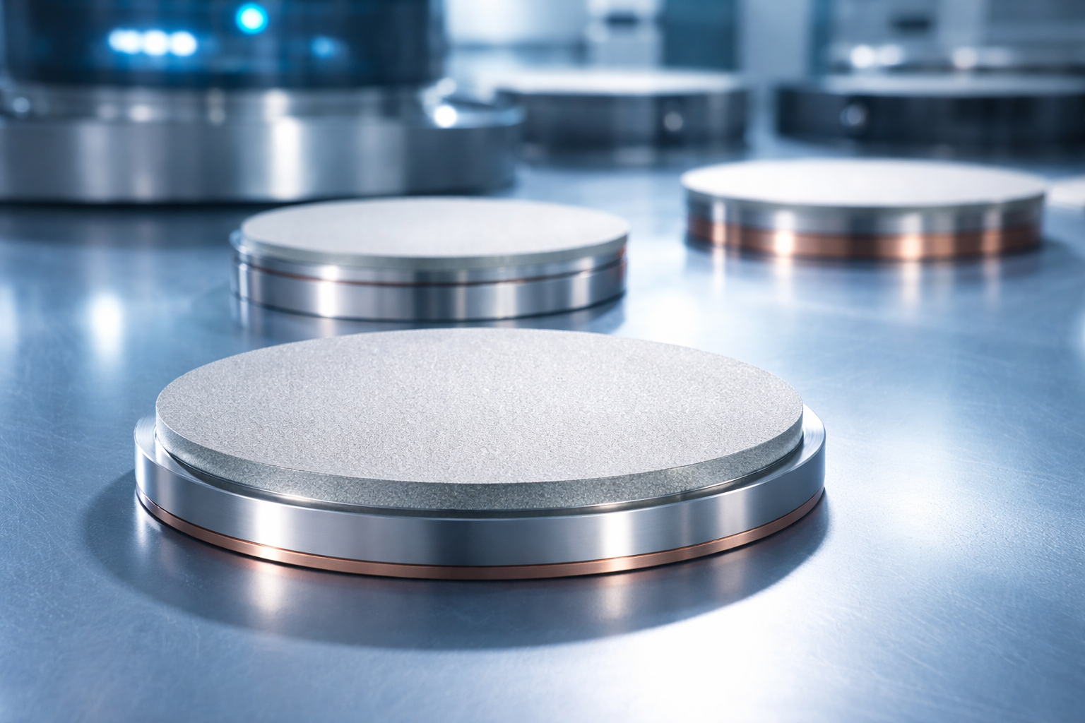
Technical Parameters of Titanium Silicate Sputtering Targets
| Parameter | Typical Value / Range | Importance |
|---|---|---|
| Composition | TiO₂–SiO₂ (custom ratios) | Determines optical & electrical properties |
| Purity | 99.9% – 99.99% | Reduces contamination in thin films |
| Density | ≥ 95% theoretical density | Ensures stable sputtering performance |
| Diameter | 25 – 300 mm (custom) | Fits various sputtering systems |
| Thickness | 3 – 8 mm | Affects target lifetime |
| Bonding | Indium / Elastomer / None | Improves heat dissipation |
Comparison with Related Materials
| Material | Key Advantage | Typical Application |
|---|---|---|
| Titanium Silicate | Tunable refractive index & stability | Optical coatings, semiconductors |
| Silicon Dioxide (SiO₂) | Excellent insulation, low cost | Dielectric layers |
| Titanium Dioxide (TiO₂) | High refractive index | Optical coatings |
| Aluminum Oxide (Al₂O₃) | High hardness & chemical resistance | Protective coatings |
Titanium silicate stands out by offering a balance between optical performance and mechanical stability.
Manufacturing Challenges and Solutions
Producing high-quality titanium silicate sputtering targets is not trivial. Key challenges include:
1. Composition Uniformity
Maintaining a consistent Ti:Si ratio throughout the target is critical to ensure uniform film properties.
2. Density Control
Low-density targets can lead to poor sputtering performance and particle generation. Advanced sintering techniques are required to achieve high density.
3. Crack Prevention
Mixed oxide ceramics can be brittle. Proper thermal management during manufacturing helps prevent cracking.
Experienced manufacturers use controlled powder processing, hot pressing, or HIP (Hot Isostatic Pressing) to address these issues.
FAQ
| Question | Answer |
|---|---|
| Can titanium silicate targets be customized? | Yes, composition ratios, size, and bonding options can be tailored to specific applications. |
| What sputtering method is recommended? | RF magnetron sputtering is typically preferred due to the insulating nature of the material. |
| How does composition affect performance? | The Ti:Si ratio directly influences refractive index, dielectric properties, and film stress. |
| Are these targets suitable for large-area coating? | Yes, high-density targets support uniform deposition over large substrates. |
| What industries use titanium silicate most? | Semiconductor, optics, display technology, and energy industries. |
Conclusion
Titanium Silicate Sputtering Targets represent a highly versatile material solution for modern thin film Titanium Silicate Sputtering Targetsdeposition. By combining the strengths of titanium oxide and silicon dioxide, they offer a unique balance of optical tunability, chemical stability, and mechanical reliability.
For industries requiring precise control over film properties—such as semiconductors, optics, and advanced coatings—titanium silicate provides a reliable and customizable option.
For detailed specifications and a quotation, please contact us at sales@thinfilmmaterials.com.