In the rapidly advancing landscape of semiconductor manufacturing and high-frequency telecommunications, the demand for novel materials has never been more acute. Scandium Nitride (ScN) has transitioned from a laboratory curiosity to a cornerstone of modern vacuum deposition. As a transition-metal nitride with a unique rock-salt crystal structure, ScN is the primary precursor for creating Aluminum Scandium Nitride (AlScN)—the material currently revolutionizing the 5G RF front-end industry.
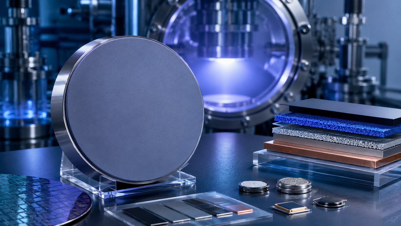
For engineers and researchers, the challenge lies in sourcing Scandium Nitride sputtering targets that offer the precise stoichiometry and ultra-low impurity levels required to achieve high-performance piezoelectric and semiconducting thin films. Thin Film Materials (TFM) provides the industry-leading purity and density necessary to drive these innovations.
1. Material Characteristics and Physical Properties
Scandium Nitride is a refractory semiconductor known for its high melting point ($~2600°C$) and significant thermal stability. Unlike traditional nitrides, ScN possesses a relatively narrow indirect bandgap, making it an intriguing candidate for both electronic and thermoelectric applications.
Table 1: Technical Specifications of TFM ScN Sputtering Targets
| Property | Value / Specification |
| Chemical Formula | ScN |
| Purity Options | 99.9% (3N), 99.95%, 99.99% (4N) |
| Theoretical Density | 4.39 g/cm³ |
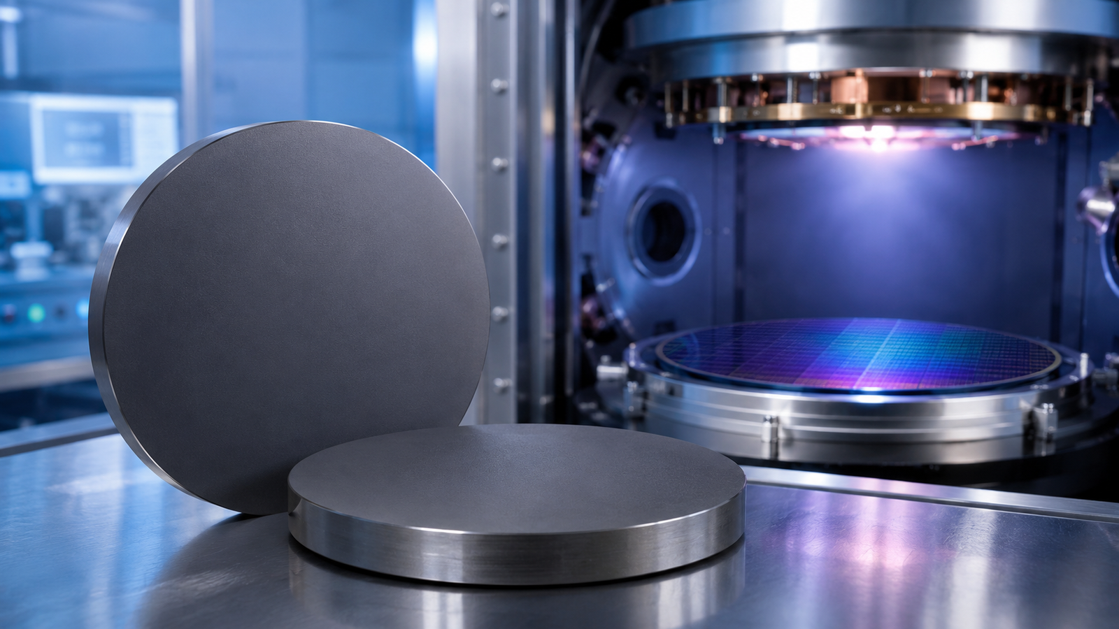
| Typical Color | Dark Grey to Black (Target form) / Orange-Yellow (Thin film) |
| Crystal Structure | Cubic (Rock-salt, B1) |
| Available Geometries | Discs, Plates, Rotatable Tubes, Custom Steps |
| Thermal Conductivity | ~10 W/(m·K) at Room Temperature |
2. Competitive Analysis: ScN vs. Conventional Nitrides
To understand why Scandium-based materials are gaining market share, it is essential to compare ScN against standard materials like Aluminum Nitride (AlN) and Titanium Nitride (TiN).
Table 2: Comparative Performance Matrix
| Feature | Scandium Nitride (ScN) | Aluminum Nitride (AlN) | Titanium Nitride (TiN) |
| Primary Role | Semiconductor/Piezoelectric Doping | Insulator/Piezoelectric | Diffusion Barrier/Hard Coating |
| Hardness (GPa) | ~21 | ~25 | ~20 |
| Electrical Behavior | n-type Semiconductor | Wide-gap Insulator | Metallic Conductor |
| Lattice Match | Excellent for GaN/SiC | Good for Sapphire | Standard for Si |
| 5G Applicability | High (As AlScN) | Moderate (Traditional) | Low |
While AlN has been the workhorse of the RF filter industry (BAW/SAW filters) for decades, the addition of Sc from an ScN source enhances the electromechanical coupling coefficient ($k^2$) by up to ten times, allowing for the wider bandwidths required by 5G and 6G protocols.
3. Key Applications Driving Demand
The adoption of PVD sputtering targets composed of Scandium Nitride is largely driven by three critical sectors:
A. RF Front-End and 5G/6G Communication
The most significant growth area is the production of AlScN thin films. By co-sputtering ScN with Aluminum or using a composite AlSc alloy target, manufacturers can create filters that handle higher frequencies and steeper rejection bands. This is vital for smartphones and infrastructure operating in the sub-6GHz and mmWave spectrums.
B. Ferroelectric Nitride Semiconductors
Recent breakthroughs have demonstrated that ScN-doped III-nitrides exhibit ferroelectric properties. This allows for the development of non-volatile memory devices that are compatible with existing GaN technology, potentially leading to “all-nitride” integrated circuits for aerospace and automotive power electronics.
C. Thermoelectrics and Optoelectronics
Due to its high power factor and ability to withstand extreme temperatures, ScN is used in the development of thermoelectric generators. Furthermore, its lattice matching with Gallium Nitride makes it an excellent buffer layer for LED and Laser Diode production, reducing dislocation density and improving device longevity.
4. Overcoming Manufacturing Challenges: The TFM Advantage
Sputtering ScN is notoriously difficult due to its brittle nature and sensitivity to oxygen contamination. Low-quality targets often suffer from “nodule” formation, which leads to arcing and film defects. TFM has optimized the manufacturing process to eliminate these pain points.
Table 3: TFM Quality Standards vs. Generic Market Targets
| Quality Metric | Generic ScN Targets | TFM Premium ScN Targets |
| Relative Density | 90% – 94% | > 98% (Vacuum Hot Pressing) |
| Oxygen Content | > 2000 ppm | < 600 ppm |
| Microstructure | Coarse, non-uniform grains | Fine, equiaxed grains (< 100 μm) |
| Machining Precision | +/- 0.5 mm | +/- 0.1 mm (CNC Finish) |
| Bonding Quality | Standard Air Bonding | Ultra-High Vacuum Indium Bonding |
By utilizing Vacuum Hot Pressing (VHP) and specialized inert-gas handling, TFM ensures that every ScN target delivers a stable deposition rate and uniform film thickness across the entire substrate.
5. Technical Guidelines for Sputtering ScN
For optimal results with our materials, we recommend the following process parameters:
- Sputtering Mode: RF Sputtering is recommended due to the semiconducting nature of ScN, though Pulsed DC can be used with high-density targets to increase deposition rates.
- Atmosphere: A mix of Ar and $N_2$ (Reactive Sputtering) is often used to maintain stoichiometry, even when using a ceramic ScN target.
- Substrate Temperature: Elevating the substrate to $300°C – 700°C$ enhances the crystallinity of the ScN or AlScN film.
- Target Cooling: High-power density requires efficient water-cooled backing plates to prevent target cracking.
6. Comprehensive FAQ for Engineers and Buyers
1. What is the standard purity of TFM ScN targets?
We offer 99.9% as standard, but for semiconductor applications, our 99.99% (4N) purity is highly recommended to minimize trace metal interference.
2. Is it better to use an ScN target or an Al-Sc alloy target for AlScN films?
It depends on your equipment. Co-sputtering ScN and Al allows for precise tuning of the Sc concentration. Using an Al-Sc alloy target is simpler for single-cathode systems but offers less flexibility in stoichiometric adjustment.
3. How do you manage the brittleness of ScN?
All ScN targets are brittle by nature. TFM uses professional indium bonding to a copper backing plate to provide mechanical support and superior heat dissipation.
4. What are the typical impurities found in Scandium Nitride?
The most common impurities are Oxygen, Carbon, and Iron. TFM’s proprietary purification process specifically targets these elements to keep them below 800ppm and 100ppm respectively.
5. Can ScN be used as a hard coating?
While it has high hardness, ScN is more expensive than TiN or CrN. It is typically reserved for functional electronic properties rather than purely mechanical wear resistance.
6. What dimensions can TFM produce?
We can manufacture circular targets up to 18 inches in diameter and rectangular targets exceeding 1000mm for large-area industrial coaters.
7. Does TFM provide a Certificate of Analysis (COA)?
Yes, every shipment is accompanied by a COA detailing purity (via GDMS or ICP-OES) and density measurements.
8. How should ScN targets be stored?
ScN is slightly sensitive to moisture. We ship targets in vacuum-sealed, inert-gas-purged packaging. We recommend storing them in a desiccator or vacuum cabinet once opened.
9. What is the lead time for custom ScN orders?
Standard sizes are often in stock. Custom geometries or high-purity 4N batches typically have a lead time of 4 to 6 weeks.
10. Can I get a credit for spent target backing plates?
Yes, TFM offers a recycling and re-bonding service for your existing Cu backing plates to reduce your total cost of ownership.
Conclusion: Partner with TFM for Your Thin Film Success
The precision of your thin film is only as good as the material it originates from. As the industry moves toward 6G and advanced ferroelectric logic, the quality of your Scandium Nitride (ScN) sputtering target becomes a critical competitive advantage. TFM combines material science expertise with rigorous quality control to provide targets that deliver consistency, batch after batch.
Ready to elevate your deposition process?
Request a Technical Quote | View our Sputtering Target Catalog | Explore AlScN Solutions