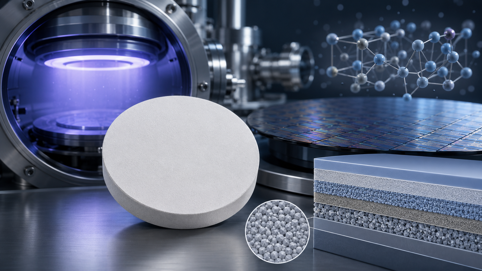
In the advanced semiconductor manufacturing and thin film deposition landscape, structural defects caused by lattice mismatch represent a persistent barrier to achieving theoretical device efficiencies. For decades, materials scientists and optoelectronic engineers developing wide-bandgap semiconductors—such as Gallium Nitride (GaN) and Zinc Oxide (ZnO)—have been forced to compromise. Depositing these materials onto traditional foreign substrates like sapphire ($\text{Al}_2\text{O}_3$) or silicon (Si) introduces severe interfacial strain, culminating in high threading dislocation densities (TDD) that degrade electrical mobility and optical performance.
ScAlMgO4 (Scandium Aluminum Magnesium Oxide), commonly designated as SAMO, fundamentally alters this paradigm. Featuring a unique layered hexagonal crystal structure, ScAlMgO4 provides a nearly flawless lattice match for ZnO and an exceptionally close match for GaN.
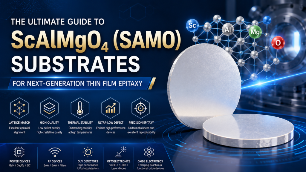
This comprehensive technical guide delivers an exhaustive analysis of the crystallographic physics of ScAlMgO4 substrates, presents horizontal performance benchmarks against legacy alternative substrates, details optimized physical vapor deposition (PVD) processing parameters, and outlines how pairing these substrates with ultra-pure thin film materials maximizes next-generation device yields.
1. Crystallographic Physics of ScAlMgO4 (SAMO)
To understand why ScAlMgO4 is uniquely suited for high-purity thin film epitaxy, one must examine its atomic architecture. SAMO is a complex oxide compound crystallizing in the rhombohedral system, mapped within the $R\bar{3}m$ space group.
The Layered Anisotropic Lattice
The crystal structure of SAMO is highly anisotropic, characterized by a distinct stacking sequence along the c-axis. It consists of alternating layers of:
- $\text{ScO}_2$ Layers: Where Scandium ($Sc^{3+}$) ions are coordinated octahedrally by Oxygen ions.
- $\text{AlMgO}_2$ Layers: Where Aluminum ($Al^{3+}$) and Magnesium ($Mg^{2+}$) ions are randomly distributed within tetrahedral sites.
This arrangement creates an extremely weak chemical bond between the adjacent layers. Consequently, the material exhibits a highly pronounced cleaving property parallel to the (0001) basal plane. By utilizing mechanical cleavage rather than aggressive chemical-mechanical polishing (CMP), engineers can reliably expose atomically flat, step-terminated surfaces that serve as pristine templates for epitaxial film growth.
Lattice Precision Metrics
The lattice constants of ScAlMgO4 are precisely defined as:
- $$a = 3.246\text{ \AA}$$
- $$c = 25.195\text{ \AA}$$
When evaluating a substrate for epitaxial configurations, the in-plane lattice constant ($a$) is the critical determinant of structural strain. The strain $\epsilon$ at the interface is calculated via the relation:
$$\epsilon = \frac{a_{\text{film}} – a_{\text{substrate}}}{a_{\text{substrate}}}$$
For a ZnO epitaxial layer ($a = 3.250\text{ \AA}$), the resulting in-plane lattice mismatch on a SAMO substrate is an astonishingly low $+0.012\%$, establishing a virtual state of homoepitaxy.
2. Horizontal Product Comparison: SAMO vs. Legacy Substrates
Selecting the correct substrate requires balancing lattice matching, thermal stability, coefficient of thermal expansion (CTE) compatibility, and total cost of ownership. The table below provides a comprehensive horizontal comparison of ScAlMgO4 substrates against standard commercial alternatives utilized for wide-bandgap semiconductor epitaxy.
Table 1: Comprehensive Horizontal Substrate Performance Matrix
| Substrate Material | Crystal Structure | Lattice Constant a ( A˚) | Mismatch with ZnO (%) | Mismatch with GaN (%) | Thermal Expansion (×10−6/K) | Typical Threading Dislocation Density (cm−2) | Primary B2B Sourcing Trade-off |
| ScAlMgO4 (SAMO) | Layered Hexagonal | 3.246 | +0.09% | -1.8% | $\alpha_a = 6.2$ $\alpha_c = 4.1$ | $< 10^5$ | Higher initial wafer cost; emerging supply chain scaling. |
| Sapphire ($\text{Al}_2\text{O}_3$) | Rhombohedral | 4.758 (30° rot: 2.747) | -18.3% | +16.0% | $\alpha_a = 7.5$ $\alpha_c = 8.5$ | $10^8 \text{ to } 10^{10}$ | Low material cost; extreme lattice mismatch requires complex buffer layers. |
| Silicon Carbide (6H-SiC) | Hexagonal | 3.081 | +5.4% | +3.5% | $\alpha_a = 4.5$ $\alpha_c = 4.2$ | $10^6 \text{ to } 10^7$ | High thermal conductivity but restricted wafer sizing and elevated cost. |
| Silicon (Si 111) | Diamond Cubic | 3.840 | +15.4% | -16.9% | $\alpha = 2.6$ | $10^9 \text{ to } 10^{10}$ | Cheapest option; severe CTE mismatch causes film cracking upon cooling. |
| Bulk GaN (Homoepitaxial) | Wurtzite | 3.189 | +1.9% | 0.0% | $\alpha_a = 5.6$ $\alpha_c = 3.2$ | $< 10^4$ | Perfect for GaN, but prohibitively expensive and unavailable in large diameters. |
3. Comprehensive Material Properties of ScAlMgO4
Engineering robust thin film architectures requires deep integration of the physical properties of the substrate into your thermal and optical design models. SAMO offers a unique combination of wide optical transparency and stable thermodynamic limits.
Table 2: Physical, Mechanical, and Optical Specifications of SAMO
| Property Category | Specific Parameter | Technical Value | Practical Impact on Thin Film Processing |
| Thermodynamic | Melting Point | ~1800°C | Enables ultra-high temperature processing during Metalorganic Chemical Vapor Deposition (MOCVD) without substrate degradation. |
| Optical | Optical Bandgap ($E_g$) | ~6.1 eV | Complete transparency down to deep UV wavelengths ($\sim 250\text{ nm}$); ideal for back-illuminated devices. |
| Refractive Index ($n$) | ~1.95 (at $\lambda = 500\text{ nm}$) | Critical for optimizing light extraction efficiency in LED and laser diode structures. | |
| Mechanical | Knoop Hardness | ~4.5 GPa | Moderate hardness permits easier mechanical dicing and laser scribing compared to sapphire. |
| Cleavage Cleanness | Perfect on (0001) | Yields atom-step profiles directly upon cleaving, eliminating subsurface damage from mechanical polishing. | |
| Electrical | Dielectric Constant ($\epsilon$) | ~10 to 12 | Provides reliable electrical isolation for high-frequency, high-electron-mobility transistors (HEMTs). |
4. Thin Film Deposition Dynamics on ScAlMgO4 Substrates
Achieving a high-purity, low-defect epilayers on a SAMO wafer requires careful management of the deposition environment. The surface kinetics of ScAlMgO4 interact directly with the kinetic energy of incoming target atoms during physical vapor deposition.
Minimizing Threading Dislocations
When film growth is initiated on a highly mismatched substrate like sapphire, the initial atomic monolayers form via island growth (Volmer-Weber mechanism). As these misaligned islands coalesce, they form structural boundaries that propagate upward as threading dislocations.
Because SAMO minimizes this initial strain energy, film growth transitions smoothly into a layer-by-layer mode (Frank-van der Merwe mechanism). This prevents the nucleation of misfit dislocations at the heterointerface, preserving the native carrier mobility of the film.
PVD Process Window Optimization
When executing RF magnetron sputtering or pulsed laser deposition (PLD) on SAMO, processing temperatures and gas ratios must be tailored to maintain stoichiometry. The table below details optimized process windows for depositing wide-bandgap films using high-performance sputtering targets.
Table 3: Process Windows for High-Purity PVD on ScAlMgO4 Substrates
| Target Material Used | Deposition Method | Optimal Substrate Temp (Ts) | Working Gas Composition | Working Pressure Range | Resulting Film Functionality |
| Zinc Oxide (ZnO) | RF Sputtering | 550°C – 650°C | Pure $\text{Ar}$ or $\text{Ar/O}_2$ (90:10) | 0.5 – 1.2 Pa | High-mobility transparent conductive oxides; piezoelectric layers. |
| Gallium Oxide ($\text{Ga}_2\text{O}_3$) | RF / Pulsed DC | 600°C – 750°C | $\text{Ar/O}_2$ (95:5) | 0.3 – 0.8 Pa | Ultra-wide bandgap power switching channels; solar-blind UV detectors. |
| High-Purity Aluminum (Al) | DC Sputtering | 200°C – 400°C | Pure $\text{Ar}$ | 0.2 – 0.5 Pa | Seed layers for AlN growth or low-resistance ohmic contact metallization. |
5. Aligning Precursor Purity with Substrate Excellence
Utilizing an premium substrate like ScAlMgO4 yields minimal benefit if the deposition flux introduces chemical contaminants or non-stoichiometric phases. To prevent the degradation of the crystalline structure at the epitaxial interface, thin film engineers must source matching evaporation materials and targets synthesized to rigorous purity and density standards.
Thin Film Materials (TFM) addresses this operational challenge by supplying co-engineered deposition portfolios designed to complement advanced complex oxide substrates.
Table 4: TFM High-Purity Precursor Specifications for SAMO Epitaxy
| Material Name & Composition | Certified Purity Level | Form Factor Options | Analytical Verification Method | Direct TFM Catalog Link |
| Zinc Oxide (ZnO) | 99.999% (5N) | Planar & Rotary Targets | GDMS / ICP-OES | ZnO Sputtering Targets |
| Gallium Oxide ($\text{Ga}_2\text{O}_3$) | 99.999% (5N) | Pellets, Granules, Targets | X-ray Fluorescence (XRF) | Evaporation Materials |
| Metallic Gallium (Ga) | 99.9999% (6N) | Liquid/Solid Ingot | Glow Discharge Mass Spectrometry | High-Purity Metals |
| Magnesium Oxide (MgO) | 99.99% (4N) | Sputtering Targets | ICP-MS | Sputtering Targets |
6. Key Commercial & Industrial Applications
The integration of ScAlMgO4 substrates into mass manufacturing lines unlocks significant performance gains across several multi-billion-dollar electronic sectors.
High-Power & High-Frequency GaN Power Electronics
In high-electron-mobility transistors (HEMTs), threading dislocations act as severe charge trapping centers, accelerating premature device breakdown and exacerbating drain-lag issues. Growing GaN on SAMO reduces these dislocation paths, allowing power electronics to operate reliably near their theoretical breakdown voltages under high thermal loads.
High-Efficiency Optoelectronics (LEDs & LDs)
In standard green, blue, and UV light-emitting diodes (LEDs), structural defects cause non-radiative recombination, transforming electrical current into waste heat rather than photons. SAMO substrates substantially improve internal quantum efficiency (IQE), lowering thermal dissipation demands and increasing the lumen output per square millimeter of die area.
ZnO-Based Quantum Structures
Due to its near-zero lattice mismatch, SAMO serves as the premier substrate for cultivating high-mobility ZnO/MgZnO heterostructures. These configurations enable the observation of the quantum Hall effect and support the development of next-generation transparent transistors and advanced acoustic wave filters.
7. The TFM Advantage: Engineering Integrity from Substrate to Film
Thin Film Materials (TFM) stands as a foundational partner for advanced semiconductor R&D laboratories and industrial scale-up facilities. We recognize that sub-nanometer anomalies at the interface can compromise entire production runs.
- Epi-Ready Cleavage Precision: Our ScAlMgO4 wafers are handled in class-100 cleanrooms and cleaved to ensure atom-step precision ($R_a < 0.2\text{ nm}$), making them ready for immediate loading into MBE or MOCVD cluster tools.
- Target Density Optimization: TFM’s oxide targets (such as $\text{ZnO}$ and $\text{Ga}_2\text{O}_3$) undergo specialized Hot Isostatic Pressing (HIP). This achieves relative densities $>99\%$, significantly reducing micro-arc events and particle spitting during prolonged PVD runs.
- Traceable Analytics: Every shipment is accompanied by detailed X-ray Diffraction (XRD) rocking curves to verify crystal orientation, alongside comprehensive mass spectrometry profiles establishing chemical purity.
8. Conclusion & Actionable Call to Action
ScAlMgO4 (SAMO) substrates resolve long-standing material constraints in wide-bandgap semiconductor manufacturing. By eliminating structural lattice strain, SAMO minimizes threading dislocation densities, unlocking the full performance potential of GaN and ZnO thin film architectures.
To maximize the benefits of this substrate technology, pairing it with ultra-pure, high-density deposition precursors is essential. TFM provides the end-to-end material pipeline required to support your next breakthrough from initial prototyping to high-volume commercial manufacturing.
Are you ready to optimize your epitaxial film properties and improve device yields? Contact our technical engineering team today to request a quote for custom-dimensioned SAMO wafers and matched sputtering targets.
Request a Quote for ScAlMgO4 Substrates & Sputtering Targets
9. Frequently Asked Questions (FAQ)
1. Why does ScAlMgO4 split so easily along the (0001) plane?
The atomic bonding between the alternating $\text{ScO}_2$ and $\text{AlMgO}_2$ layers is governed by weak electrostatic and van der Waals forces. This structural characteristic allows the crystal to cleave easily along its basal plane, producing a pristine surface without the subsurface damage typical of mechanical grinding.
2. Can I use SAMO substrates in conventional MOCVD systems?
Yes. SAMO is highly compatible with Metalorganic Chemical Vapor Deposition (MOCVD) systems. With a melting point near 1800°C, it remains completely stable at typical growth temperatures ($600^{\circ}\text{C} – 1100^{\circ}\text{C}$) under ammonia ($\text{NH}_3$) or oxygen processing atmospheres.
3. How does the thermal expansion coefficient (CTE) of SAMO compare to GaN?
SAMO features an in-plane CTE ($\alpha_a$) of $6.2 \times 10^{-6}/\text{K}$, closely matching that of GaN ($5.6 \times 10^{-6}/\text{K}$). This close thermal match prevents the micro-cracking and wafer bowing that frequently occur when cooling thick GaN layers grown on silicon or sapphire.
4. What are the typical dimensions of SAMO substrates supplied by TFM?
TFM supplies standard 1-inch and 2-inch diameter circular wafers, along with common square dimensions ($10 \times 10\text{ mm}$ and $20 \times 20\text{ mm}$). Custom geometries and off-cut angle orientations are also available upon request to meet specific research or production needs.
5. Does the material exhibit absorption in the ultraviolet (UV) spectrum?
No. Thanks to its wide optical bandgap of approximately 6.1 eV, ScAlMgO4 maintains high optical transparency ($>80\%$) across both the visible spectrum and into the deep ultraviolet region down to roughly 250 nm. This makes it an ideal platform for back-illuminated UV photodetectors.
6. Is it necessary to perform chemical-mechanical polishing (CMP) on an epi-ready SAMO substrate?
No. TFM’s SAMO substrates are delivered with “epi-ready” surfaces. Because they are prepared via precision mechanical cleavage along the native atomic planes, they exhibit sub-nanometer surface roughness ($R_a < 0.2\text{ nm}$) and require no further polishing prior to deposition.
7. What pre-deposition chamber cleaning cycle is recommended for SAMO?
To preserve the atomic step structure, we recommend a non-aggressive thermal degassing cycle within the vacuum chamber ($400^{\circ}\text{C} – 500^{\circ}\text{C}$ under ultra-high vacuum or a light oxygen flow). Avoid harsh, concentrated acid dips unless your process has been specifically calibrated for them.
8. Does TFM provide backing plate bonding for the oxide targets used with SAMO?
Yes. For brittle ceramic targets like Zinc Oxide ($\text{ZnO}$) or Gallium Oxide ($\text{Ga}_2\text{O}_3$), TFM offers professional metallic indium bonding services to high-conductivity copper backing plates. This ensures uniform cooling and prevents thermal cracking during high-power RF sputtering runs.
9. What is the typical threading dislocation density (TDD) of ZnO grown on SAMO?
While ZnO grown on legacy sapphire typically exhibits a TDD between $10^8$ and $10^{10}\text{ cm}^{-2}$, homoepitaxial-like growth on a SAMO substrate routinely achieves a TDD below $10^5\text{ cm}^{-2}$, as verified by transmission electron microscopy (TEM).
10. How can I get pricing for bulk procurement or specialized research designs?
You can submit your required technical specifications—including dimensions, thickness, quantity, and any custom orientation requirements—directly via our secure interface at TFM Contact Page. Our sales engineering team will generate a comprehensive technical quotation within 24 business hours.