The Bottleneck in Silicon Photonics: Optical Isolation
The rapid expansion of 5G, cloud computing, and massive data centers has pushed traditional electronic circuits to their physical limits. Enter Photonic Integrated Circuits (PICs), which use photons instead of electrons to process and transmit information at the speed of light. While silicon photonics has successfully miniaturized lasers, modulators, and detectors onto single semiconductor chips, one critical component has stubbornly resisted integration: the optical isolator.
Optical isolators act as “one-way valves” for light, preventing back-reflected signals from returning to the laser source and causing phase noise, mode-hopping, or catastrophic damage. Traditionally, these isolators rely on bulky, discrete crystals that cannot be easily integrated into a planar chip architecture.
Overcoming this bottleneck requires advanced magneto-optical thin films, specifically those deposited using high-purity sputtering targets. Today, the definitive material solving this challenge is Bismuth-substituted Yttrium Iron Garnet (BiY₂Fe₅O₁₂ or Bi-YIG).
Enter Bismuth-Substituted YIG (Bi-YIG)
To achieve non-reciprocal light transmission on a microscopic scale, engineers rely on the Faraday effect—the rotation of the polarization plane of light as it passes through a material in the presence of a magnetic field.
Why Pure YIG Falls Short for PICs
Pure Yttrium Iron Garnet (Y₃Fe₅O₁₂) is legendary in microwave engineering for its ultra-low acoustic loss. However, its specific Faraday rotation in the near-infrared telecom wavelengths (1310 nm and 1550 nm) is relatively weak. To achieve the necessary 45-degree polarization rotation for an isolator using pure YIG, the thin film would need to be impractically thick, defeating the purpose of miniaturized PICs.
The Giant Faraday Effect of BiY₂Fe₅O₁₂
By replacing certain Yttrium ions in the garnet lattice with heavier Bismuth ions, material scientists created BiY₂Fe₅O₁₂. This substitution drastically enhances the spin-orbit coupling of the iron ions, resulting in a Giant Faraday Rotation that is orders of magnitude stronger than pure YIG.
This massive enhancement allows engineers to achieve the necessary polarization rotation within a film thickness of just a few micrometers. Utilizing high-density BiY2Fe5O12 sputtering targets, telecom engineers can finally fabricate monolithic, on-chip optical isolators that seamlessly integrate with standard silicon waveguides.
Table 1: Horizontal Material Comparison – Magneto-Optical Candidates for PICs
To understand why Bi-YIG dominates PIC applications, compare it against pure YIG and Terbium Gallium Garnet (TGG), the traditional bulk isolator material.
| Feature / Metric | Bi-YIG (BiY₂Fe₅O₁₂) | Pure YIG (Y₃Fe₅O₁₂) | TGG (Tb₃Ga₅O₁₂) |
| Faraday Rotation (@ 1550nm) | Extremely High (Giant) | Low | Moderate |
| Suitability for Thin Film / PICs | Excellent (Micro-scale) | Poor (Requires thick films) | Poor (Used mainly as bulk crystals) |
| Optical Absorption Loss | Moderate (Manageable) | Very Low | Very Low |
| Target Deposition Method | RF Magnetron Sputtering | RF Magnetron Sputtering | Bulk Crystal Growth |
| Primary Application | On-chip integrated isolators | Microwave filters, Magnonics | Free-space, high-power lasers |
Key Applications of Bi-YIG in Telecommunications
The deposition of complex oxides like Bi-YIG is not limited to a single component. As the telecom industry moves toward fully integrated photonics, Bi-YIG thin films are enabling a suite of advanced devices.
Table 2: PIC Components Leveraging Bi-YIG Thin Films
| Telecom Component | Function in the Circuit | How Bi-YIG Enables It |
| Integrated Optical Isolators | Protects on-chip DFB/DBR lasers from back-reflections. | Provides non-reciprocal 45° polarization rotation in a compact footprint. |
| Optical Circulators | Routes bi-directional light signals into separate distinct ports. | High magneto-optic figure of merit allows complex routing without massive signal loss. |
| Magneto-Optic Modulators | Modulates light intensity or phase via an external magnetic field. | Fast response time and strong magnetic coupling enable high-speed data encoding. |
| Photonic Sensor Arrays | Detects minute changes in localized magnetic fields. | Giant Faraday effect allows for highly sensitive, miniaturized magnetic field mapping. |
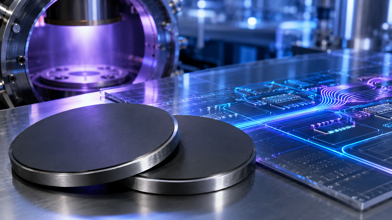
PVD Challenges: Sputtering BiY₂Fe₅O₁₂ Thin Films
Fabricating these integrated devices requires translating the bulk properties of BiY₂Fe₅O₁₂ into a pristine thin film. Because Bi-YIG is an insulating ceramic, Radio Frequency (RF) Magnetron Sputtering is the industry standard Physical Vapor Deposition (PVD) method.
However, optical engineers face three primary challenges during deposition:
- Bismuth Volatility: Bismuth evaporates at much lower temperatures than Yttrium or Iron. During high-temperature sputtering or post-deposition rapid thermal annealing (RTA), Bismuth loss can ruin the film’s stoichiometry.
- Phase Crystallization: Films deposited at room temperature are amorphous and lack magneto-optical properties. They must be annealed (typically 650°C – 800°C) to form the necessary garnet crystal structure.
- Lattice Mismatch: Growing Bi-YIG directly on Silicon causes thermal stress and cracking. Engineers often use buffer layers (like CeO₂ or Y₂O₃) or specialized substrates like Gadolinium Gallium Garnet (GGG).
Table 3: Optimization Parameters for RF Magnetron Sputtering of Bi-YIG
| Sputtering Parameter | Typical Optimization Range | Engineering Rationale |
| Sputtering Source | RF Power (13.56 MHz) | Essential to prevent charging and severe arcing on the insulating Bi-YIG ceramic target. |
| Working Gas Atmosphere | Ar + O₂ (typically 10-20% O₂) | Reactive sputtering compensates for oxygen loss in the plasma, preventing oxygen vacancies in the film. |
| Substrate Temperature | Room Temp (followed by RTA) OR 600°C+ | Heating drives crystalline phase formation. Post-deposition RTA is often preferred to minimize prolonged Bismuth evaporation. |
| Target Stoichiometry | Bi-rich (Customized) | Sputtering targets are intentionally formulated with excess Bismuth to compensate for thermal loss during deposition and annealing. |
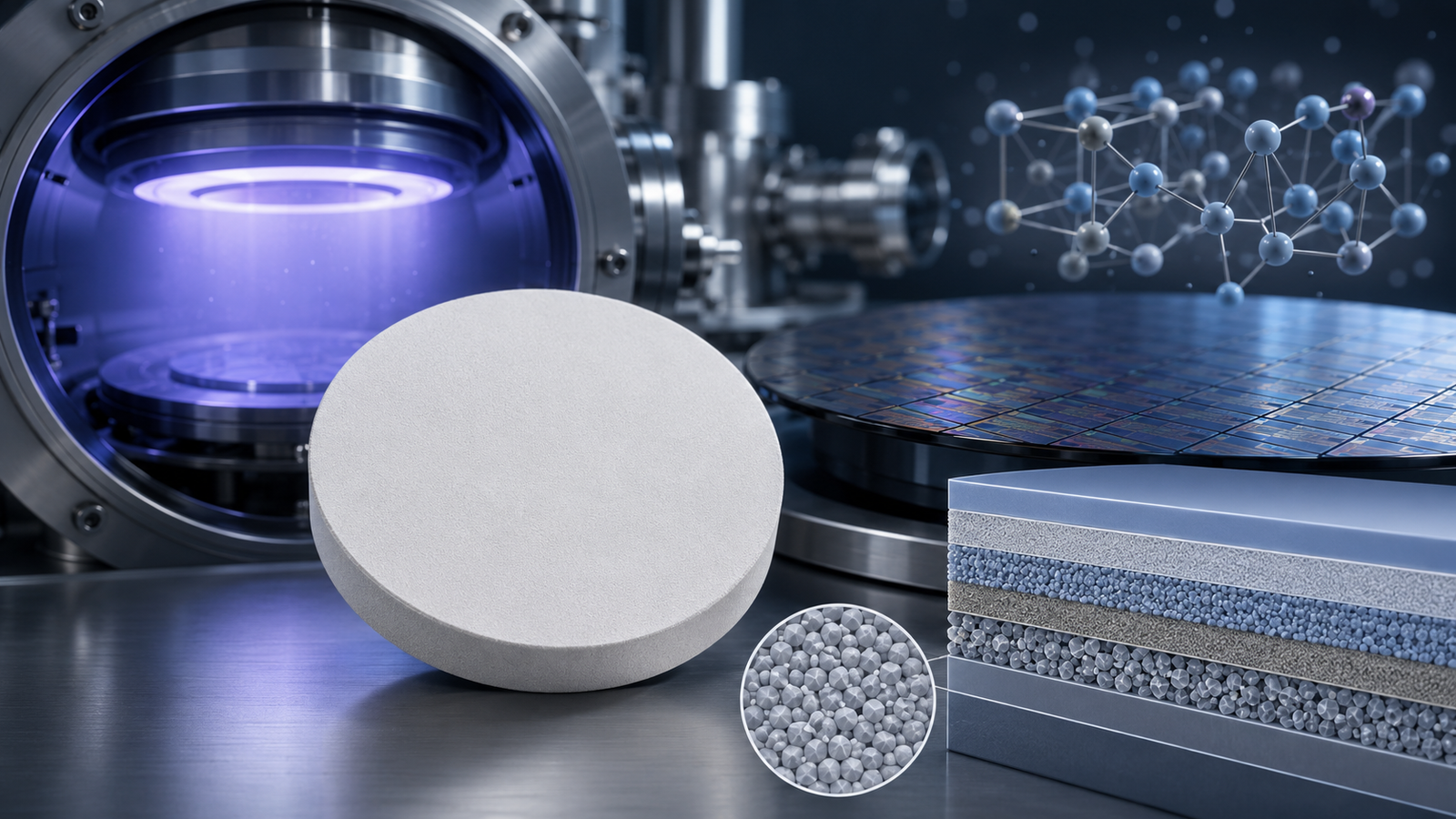
The TFM Advantage: High-Density Bi-YIG Sputtering Targets
The success of your photonic integration heavily depends on the quality of your source material. Substandard Bi-YIG targets with low density or improper stoichiometry will result in particulate contamination, unstable plasmas, and weak Faraday rotation in your final devices.
At Thin Film Materials (TFM), we engineer custom sputtering targets specifically tailored for advanced photonics and telecom research:
- Optimized Stoichiometry: We can adjust the Bismuth-to-Yttrium ratio (e.g., Bi₁Y₂Fe₅O₁₂, Bi₂Y₁Fe₅O₁₂) or provide Bismuth-enriched targets to perfectly compensate for your system’s specific thermal evaporation rates.
- Ultra-High Density: Manufactured using advanced Hot Isostatic Pressing (HIP), our ceramic targets achieve >95% relative density. This eliminates void-induced micro-arcing and significantly reduces nodule formation.
- Expert Bonding Services: To prevent thermal shock and target cracking during RF sputtering, all our Bi-YIG targets can be securely bonded to OFHC copper backing plates using proprietary elastomer or Indium bonding techniques.
Conclusion
Photonic Integrated Circuits are the future of high-speed telecommunications, and solving the optical isolation bottleneck is the key to unlocking their full potential. By leveraging the Giant Faraday effect of Bismuth-substituted YIG, engineers can integrate high-performance isolators directly onto silicon platforms. Achieving this requires mastering RF magnetron sputtering and utilizing source materials of uncompromising quality.
Don’t let subpar materials limit your photonic innovations.
Contact TFM today to request a quote on our high-density BiY₂Fe₅O₁₂ sputtering targets and accelerate your PIC development.
Frequently Asked Questions (FAQ)
1. Why is Bismuth used to substitute Yttrium in YIG targets?
Substituting Yttrium with Bismuth significantly increases the spin-orbit coupling within the crystal lattice. This results in the “Giant Faraday Effect,” increasing the material’s ability to rotate the polarization of light by orders of magnitude compared to pure YIG, which is essential for micro-scale optical isolators.
2. Can I deposit Bi-YIG directly onto bare Silicon substrates?
It is highly challenging due to the large lattice mismatch and differences in thermal expansion coefficients between Bi-YIG and Silicon, which causes cracking and prevents proper crystallization. Engineers typically use buffer layers (like Silicon Dioxide or Cerium Oxide) or specialized wafer bonding techniques.
3. What is the biggest challenge when sputtering BiY₂Fe₅O₁₂?
Maintaining strict stoichiometry. Bismuth is highly volatile and easily evaporates away during high-temperature deposition or post-annealing, leading to the formation of secondary phases (like Iron Oxide) that destroy the film’s magneto-optical properties.
4. How does TFM help solve the Bismuth volatility problem?
TFM can manufacture custom sputtering targets with a deliberately Bismuth-rich stoichiometry. By adding excess Bismuth to the target, we compensate for the amount lost in the vacuum chamber, ensuring your final thin film has the exact desired Bi:Y:Fe ratio.
5. Do I need to use reactive oxygen sputtering for Bi-YIG?
Yes. Although the target is an oxide, oxygen atoms are light and easily pumped out of the chamber by the turbomolecular pump. Sputtering in an Argon/Oxygen mixture (usually 10% to 20% O₂) prevents oxygen vacancies, which can negatively impact the film’s optical transparency.
6. Why must I use RF power instead of DC power for Bi-YIG?
BiY₂Fe₅O₁₂ is an insulating ceramic complex oxide. If you apply DC power, positive Argon ions will accumulate on the target surface, stopping the sputtering process and eventually causing massive electrical arcs that will crack the target and damage your power supply.
7. Why do my as-deposited Bi-YIG films show no Faraday rotation?
Films sputtered at room temperature are amorphous. The magneto-optical properties of Bi-YIG depend entirely on its specific garnet crystal lattice. You must perform a post-deposition high-temperature anneal to crystallize the film.
8. Is Rapid Thermal Annealing (RTA) better than furnace annealing for Bi-YIG?
Generally, yes. Because prolonged exposure to high heat causes Bismuth evaporation, RTA allows the film to reach crystallization temperatures (e.g., 700°C) very quickly and cool down rapidly, minimizing Bismuth loss while successfully forming the garnet phase.
9. What backing plate bonding method do you recommend for Bi-YIG targets?
Because Bi-YIG is a brittle ceramic with low thermal conductivity, it is highly susceptible to thermal shock. We strongly recommend elastomer bonding or Indium bonding to an Oxygen-Free High Conductivity (OFHC) copper backing plate to ensure maximum heat dissipation.
10. Can TFM supply other doped YIG materials for PIC research?
Yes. In addition to Bismuth-substituted YIG, TFM can custom-manufacture Cerium-substituted YIG (Ce-YIG), Gallium-substituted YIG (Ga-YIG), and Terbium Gallium Garnet (TGG) targets to suit specific Faraday rotation and wavelength requirements.