In the rapidly advancing fields of optoelectronics, smart architecture, and uncooled thermal imaging, materials engineers are constantly pushing the boundaries of transition metal oxides. Among these complex materials, Vanadium Dioxide stands out as a revolutionary candidate due to its extraordinary, reversible structural phase change. For B2B manufacturers and research institutions developing next-generation thermochromic smart windows, ultrafast optical switches, and high-sensitivity microbolometers, synthesizing stable, stoichiometric films is a critical operational imperative.
However, achieving high-quality Vanadium Dioxide thin films via Physical Vapor Deposition (PVD) or Chemical Vapor Deposition (CVD) presents significant thermodynamic and metallurgical challenges. Vanadium is a multivalent transition metal capable of forming numerous stable oxide phases, including V2O3, V2O5, and the highly sought-after VO2. A fraction of a percent deviation in oxygen partial pressure during the deposition process can yield a film with completely different electrical and optical properties.
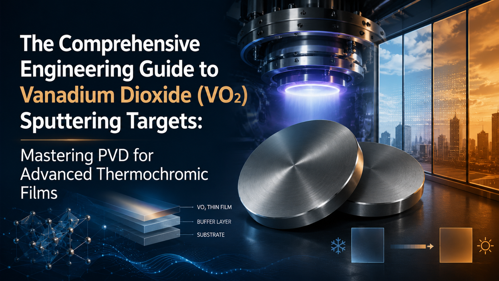
This comprehensive technical guide, brought to you by Thin Film Materials (TFM), delves deeply into the physics of Vanadium Dioxide, compares it horizontally against other smart coating materials, outlines optimized magnetron sputtering parameters, and explains why sourcing high-density, high-purity sputtering targets is the foundational step for guaranteeing process repeatability and commercial viability.
The Physics and Thermodynamics of Vanadium Dioxide
To understand the stringent requirements placed on the PVD process, engineers must first understand the solid-state physics that dictates the behavior of Vanadium Dioxide.
The Metal-Insulator Transition (MIT) Mechanism
The defining characteristic of Vanadium Dioxide is its reversible Metal-Insulator Transition (MIT), which occurs near a critical temperature (Tc) of approximately 68°C (341 K). This transition is classified as a first-order phase transition characterized by a massive, abrupt change in the material’s electrical resistivity and optical transmittance.
- Below 68°C (The Insulating Phase): At room temperature, VO2 exists in a monoclinic crystal structure. In this state, it acts as a semiconductor with a bandgap of approximately 0.6 eV. Optically, monoclinic VO2 is highly transparent to infrared (IR) radiation. In architectural applications, this allows solar thermal energy to pass through the glass, passively warming the interior of a building.
- Above 68°C (The Metallic Phase): As the material is heated past its critical temperature, the atomic lattice undergoes a structural rearrangement into a highly symmetric rutile (tetragonal) phase. This phase shift causes the valence and conduction bands to overlap, transforming the material into a metal. Optically, it becomes highly reflective to near-infrared and mid-infrared wavelengths while maintaining its visible light transmittance. This effectively blocks solar heat gain, significantly reducing the energy load on air conditioning systems.
This phenomenon is driven by a complex interplay of electron-electron correlations (the Mott-Hubbard transition) and lattice distortions (the Peierls transition). Because this transition is strictly temperature-dependent and entirely passive, VO2 offers a massive engineering advantage over complex active systems that require continuous electrical biasing.
Horizontal Comparative Analysis of Smart Coating Materials
When designing smart glass architectures or thermal sensing arrays, engineering teams must evaluate multiple transition metal oxides and transparent conductive oxides. To make an informed, data-driven decision, it is essential to compare Vanadium Dioxide horizontally against other industry-standard materials.
Table 1: Horizontal Comparison of Smart Window and Sensor Thin Film Materials
| Material Specification | Vanadium Dioxide (VO2) | Tungsten Oxide (WO3) | Indium Tin Oxide (ITO) | Vanadium Pentoxide (V2O5) |
| Primary Mechanism | Thermochromic (Temperature) | Electrochromic (Voltage Bias) | Static Low-E (No Phase Change) | Electrochromic / Ion Intercalation |
| Phase Transition Trigger | ~68°C (Tunable via W-doping) | Applied Electrical Current | N/A | Applied Voltage & Li+ Ions |
| Optical Modulation Target | Infrared (IR) Wavelengths | Visible Light Wavelengths | Static IR Blocking | Visible and Near-IR |
| Coating System Complexity | Low: Single active functional layer | High: Requires 5+ structural layers | Low: Single or dual layer | High: Requires liquid/solid electrolyte |
| Typical Response Time | Ultrafast (Femtoseconds in photonics) | Slow (Seconds to minutes for large areas) | Instant (Static characteristic) | Moderate (Seconds) |
| Preferred PVD Technique | RF Sputtering / Pulsed DC | Reactive DC Sputtering | DC Magnetron Sputtering | RF / DC Sputtering |
| Commercial Applications | Passive Smart Glass, Microbolometers | Active Dimming Glass, Mirrors | Touchscreens, Solar Cells | Advanced Battery Cathodes |
Engineering Insight: While Tungsten Oxide (WO3) allows users to manually control the tint of an architectural window, it necessitates a highly complex, multi-layered device structure including transparent conductive electrodes (like ITO), an ion-storage layer, and an active electrolyte layer. Vanadium Dioxide, conversely, functions autonomously as a single active layer. This drastically lowers manufacturing complexity, reduces thin-film stress, and limits the overall bill of materials for B2B glass manufacturers.
Physical Vapor Deposition (PVD) Challenges for VO2
Synthesizing a pure, crystalline, and stoichiometric VO2 film without inadvertently creating V2O3 or V2O5 impurities requires absolute mastery over thin film deposition parameters. Process engineers generally navigate between two primary sputtering methodologies: Reactive DC Sputtering and RF/Pulsed DC Sputtering.
Managing the Hysteresis Loop in Reactive DC Sputtering
In this approach, a pure metallic Vanadium target (99.95% or higher) is sputtered in a vacuum chamber containing a precisely controlled mixture of Argon (working gas) and Oxygen (reactive gas). The primary challenge here is the well-documented “hysteresis effect” of reactive sputtering.
- Metallic Mode: If the oxygen flow is too low, the process operates in the metallic mode, depositing an opaque, metallic Vanadium film that exhibits no phase transition.
- Poisoned Mode: If the oxygen flow is too high, the surface of the Vanadium target becomes heavily oxidized (target poisoning). The sputtering yield plummets, deposition rates drop drastically, and the resulting film is typically over-oxidized V2O5, which lacks the desired MIT properties.
- Transition Mode: To deposit stoichiometric VO2, the process must be maintained in the incredibly narrow “transition mode” located on the steep slope of the hysteresis curve. This requires highly sophisticated closed-loop control systems, such as Plasma Emission Monitoring (PEM), to dynamically adjust the oxygen partial pressure in milliseconds.
RF Sputtering from Ceramic VO2 Targets
To bypass the severe instabilities of the reactive hysteresis loop, many R&D laboratories and high-yield manufacturing facilities prefer to sputter directly from a pre-synthesized ceramic Vanadium Dioxide (VO2) sputtering target. Because the target already possesses the correct VO2 stoichiometry, the deposition process is inherently more stable.
However, ceramic VO2 is a semiconductor/insulator at room temperature. Utilizing standard DC power will result in positive charge accumulation on the target surface, leading to catastrophic electrical arcing, plasma extinguishment, and particulate ejection. Therefore, Radio Frequency (RF) or advanced Pulsed DC power supplies are strictly required to discharge the target surface during deposition.
The Critical Role of Substrate Temperature
The thermodynamic formation of the desired monoclinic/rutile VO2 phase requires significant thermal activation energy. If VO2 is sputtered onto an unheated substrate at room temperature, the resulting film will be entirely amorphous and will not exhibit the Metal-Insulator Transition.
To achieve crystallization, the substrate must be heated in-situ to temperatures ranging between 400°C and 550°C during deposition. Alternatively, engineers can deposit amorphous films at lower temperatures and subject them to a rigorous post-deposition thermal annealing process in a precisely controlled ambient environment (often a specific mix of Argon and trace Oxygen) to induce crystallization without over-oxidizing the film.
Process Optimization and Starting Sputtering Parameters
To assist your engineering team in accelerating the R&D phase and establishing a stable baseline, TFM provides the following starting parameters for utilizing our high-density ceramic VO2 targets in a standard high-vacuum magnetron system.
Table 2: Recommended Starting Parameters for RF Sputtering of Ceramic VO2
| Process Parameter | Recommended Operational Range | Technical Justification and Impact |
| Power Supply Type | 13.56 MHz RF or Pulsed DC (20-100 kHz) | Neutralizes positive argon ions on the insulating ceramic surface, preventing arc generation. |
| Target Power Density | 2.0 W/cm² – 4.0 W/cm² | Limits thermal shock. Exceeding this density can cause the brittle ceramic target to crack due to inadequate heat dissipation. |
| Base Pressure | < $5.0 \times 10^{-6}$ Torr | Removes residual water vapor and atmospheric contaminants that can inadvertently alter film stoichiometry. |
| Working Pressure | 2.0 mTorr – 6.0 mTorr | Optimizes the mean free path of sputtered Vanadium and Oxygen atoms, promoting dense, conformal film growth. |
| Process Gas Mixture | Ar (Main) + 1% to 3% O2 | Even when using a stoichiometric ceramic target, trace oxygen is often required to compensate for lighter oxygen atoms lost to the vacuum pumps during transport. |
| Substrate Temperature | 450°C – 550°C | Provides the thermodynamic energy required for adatom surface mobility and in-situ formation of the crystalline monoclinic phase. |
Troubleshooting Common PVD Defects
- Defect: Yellowish Film with No Phase Transition: This indicates severe over-oxidation (formation of V2O5). Solution: Reduce the oxygen partial pressure in the gas mixture, increase the sputtering power slightly to increase the metal-to-oxygen arrival ratio, and verify the vacuum chamber has no microscopic atmospheric leaks.
- Defect: High Pinhole Density (Spitting): Macro-particles on the substrate are usually caused by a low-density target outgassing or micro-arcing. Solution: Ensure you are utilizing a high-density target (>95%) and verify that your Pulsed DC frequency is optimized for arc suppression.
- Defect: Target Cracking During Plasma Ignition: Ceramic oxides suffer from poor thermal conductivity. Rapid application of high power causes localized thermal expansion and fracturing. Solution: Ramp up the RF power at a maximum rate of 5 to 10 Watts per minute and ensure the target is bonded to a water-cooled backing plate.
Why High-Purity VO2 Sputtering Targets Matter
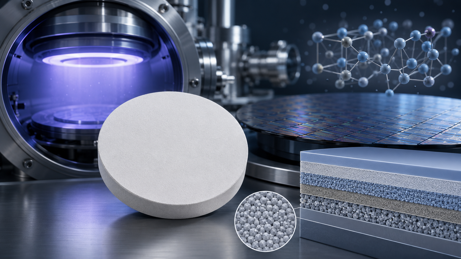
A perfectly calibrated PVD recipe is entirely negated if the source material is fundamentally compromised. The purity, theoretical density, and microstructural homogeneity of the sputtering target dictate the baseline quality, electrical performance, and defect density of the resulting thin films.
At Thin Film Materials (TFM), our metallurgical engineers employ advanced vacuum hot-pressing and vacuum sintering technologies to manufacture Vanadium Dioxide targets that meet and exceed the strictest B2B industrial standards.
The Impact of Impurities on the MIT Phase Transition
The sharpness and magnitude of the Metal-Insulator Transition are highly sensitive to crystallographic defects and elemental impurities. Trace amounts of heavy metals (such as Iron, Nickel, or Copper) act as electron scattering centers and can inadvertently alter the energy bandgap. This results in a “sluggish” phase transition with a wide hysteresis loop, reducing the optical switching efficiency of smart windows and lowering the Temperature Coefficient of Resistance (TCR) in microbolometers. TFM guarantees purities ranging from 3N (99.9%) to 4N (99.99%), certified by rigorous ICP-OES analysis, ensuring the sharpest possible thermodynamic response.
Density, Outgassing, and Yield Rates
Traditional, low-cost cold-pressed targets often suffer from high internal porosity (relative densities of 75% to 85%). During the high-energy PVD process, inert gases trapped within these microscopic pores rapidly heat and expand. This causes localized micro-explosions on the target surface, ejecting macroscopic solid particles directly onto the substrate—a phenomenon known as “spitting.” In semiconductor and sensor manufacturing, a single macro-particle can short-circuit a microbolometer pixel array, devastating overall production yields.
TFM’s proprietary hot-pressing manufacturing process eliminates internal voids, achieving theoretical densities greater than 95%. This virtually eliminates outgassing, prevents particulate ejection, and ensures a highly stable, repeatable plasma plume throughout the entire life cycle of the target.
Table 3: TFM VO2 Target Quality Matrix vs. Standard Industry Grade
| Quality Metric | Standard Commercial Grade VO2 | TFM High-Performance VO2 Target | Impact on B2B Manufacturing Process |
| Elemental Purity | 99.0% – 99.5% (2N to 2N5) | 99.9% – 99.99% (3N to 4N) | Preserves the intrinsic bandgap; ensures a massive, sharp magnitude shift in electrical resistivity. |
| Relative Density | ~80% – 85% (Cold Pressed) | > 95% (Vacuum Hot Pressed) | Eradicates spitting and micro-arcing; drastically improves usable target life and film uniformity. |
| Phase Composition | Often mixed with V2O3 and V2O5 | Phase-pure monoclinic VO2 | Eliminates the need for aggressive reactive gas compensation; stabilizes the deposition rate. |
| Cooling Methodology | Unbonded / Basic Epoxy | Indium or Elastomer Bonded to Copper | Facilitates efficient heat dissipation; allows for higher power densities and faster manufacturing throughput. |
Note: For researchers and facilities utilizing Electron Beam (E-Beam) or Thermal Evaporation systems, TFM also synthesizes high-purity evaporation materials in the form of customized VO2 pellets, pieces, and granules.
Target Bonding and Advanced Thermal Management
Given the intrinsic brittleness and exceptionally low thermal conductivity of ceramic oxides, proper thermal management during the magnetron sputtering process is non-negotiable. Bombarding a ceramic target with high-energy argon ions generates immense localized heat. If this heat is not rapidly dissipated through the water-cooled cathode, the temperature gradient across the thickness of the target will induce severe mechanical stress, ultimately causing the target to shatter and destroying the vacuum environment.
To prevent catastrophic material failure, TFM strongly mandates the use of our professional target bonding services for all ceramic VO2 targets.
- Indium Bonding: For high-power density applications, we utilize high-purity Indium solder to bond the VO2 target to an Oxygen-Free Copper (OFC) backing plate. Indium offers unparalleled thermal and electrical conductivity. However, because Indium melts at 156°C, the cooling system must be highly efficient.
- Elastomer Bonding: Due to the significant Coefficient of Thermal Expansion (CTE) mismatch between ceramic Vanadium Dioxide and copper, heating can cause the target to warp and detach from rigid solders. TFM’s advanced proprietary Elastomer bonding utilizes a silver-loaded conductive polymer that remains flexible under thermal stress. This absorbs the CTE mismatch, preventing target cracking while maintaining excellent thermal transfer.
Advanced Applications Driving Global VO2 Demand
The ability to consistently deposit high-quality Vanadium Dioxide using TFM targets is unlocking unprecedented capabilities across multiple high-growth technological sectors.
1. Thermochromic Smart Windows for Sustainable Architecture
The global push toward zero-emission buildings has positioned VO2 as a critical material for sustainable architecture. By integrating VO2 films into multi-pane glass systems, windows become autonomously adaptive to environmental weather conditions, rejecting solar infrared heat in the summer and absorbing it in the winter.
The Doping Requirement: To make this commercially viable for human comfort, the natural transition temperature of 68°C must be lowered to room temperature (~25°C to 30°C). TFM actively supports this sector by engineering custom Tungsten-doped Vanadium Dioxide (W-VO2) sputtering targets. By substituting a precise atomic percentage of Vanadium with Tungsten, the MIT temperature is lowered by approximately 20°C to 24°C per atomic percent of Tungsten, delivering a ready-to-sputter solution for smart glass manufacturers.
2. Uncooled Infrared Microbolometers
In the defense, automotive, and industrial inspection sectors, the demand for thermal imaging is skyrocketing. Traditional infrared cameras required bulky, expensive cryogenic cooling systems to reduce thermal noise. VO2 has emerged as the industry-standard sensing material for uncooled microbolometers due to its exceptionally high Temperature Coefficient of Resistance (TCR) precisely tuned near its phase transition, coupled with highly favorable 1/f noise characteristics. Sputtering highly uniform, ultra-thin VO2 films across dense sensor arrays is critical for achieving high-resolution, low-cost thermal imaging.
3. Ultrafast Optical Switches and Metamaterials
Because the phase transition in VO2 can be triggered not only by heat but also optically by ultrafast femtosecond laser pulses, it is heavily utilized in advanced photonics. The transition from a transparent dielectric to a highly reflective metal occurs on a sub-picosecond timescale, making VO2 thin films ideal candidates for high-speed optical switches, neuromorphic computing architectures, optical memory storage, and tunable metamaterial absorbers operating in the terahertz (THz) frequencies.
Conclusion: Securing Your Supply Chain with TFM
Synthesizing Vanadium Dioxide thin films that reliably exhibit a sharp, robust Metal-Insulator Transition is one of the most demanding disciplines in modern materials science. It requires an exact synchronization of thermodynamic parameters, sophisticated PVD equipment, and an uncompromising standard of raw material quality.
Do not allow sub-standard, highly porous ceramic targets to introduce instability, arcing, and particle defects into your critical manufacturing processes. Thin Film Materials (TFM) is your dedicated B2B partner, committed to advancing your R&D and industrial production capabilities with industry-leading purity, theoretical density, and bespoke metallurgical engineering.
Whether you require standard planar circular targets for academic research or large-scale multi-tile rotary targets for continuous roll-to-roll architectural glass coating, our manufacturing infrastructure is built to scale with your ambitions.
Take the next step in optimizing your deposition process.
Request a Quote today and consult directly with TFM’s materials engineering team to discuss your specific dimensional requirements, Tungsten doping concentrations, and advanced backing plate bonding solutions.
Frequently Asked Questions (FAQ)
1. What exactly triggers the Metal-Insulator Transition (MIT) in Vanadium Dioxide?
The MIT in pure VO2 is a first-order phase transition triggered primarily by temperature, occurring at approximately 68°C. It involves a simultaneous structural change from a monoclinic to a rutile crystal lattice and an electronic transition from a semiconducting state to a metallic state, drastically altering its electrical conductivity and optical transmittance in the infrared spectrum.
2. Can I deposit crystalline VO2 on a substrate at room temperature?
No. Sputtering VO2 onto an unheated substrate will result in an amorphous thin film that does not exhibit the characteristic MIT properties. You must either heat the substrate during deposition (typically between 400°C and 550°C) or perform a high-temperature post-deposition annealing process in a controlled environment to induce crystallization.
3. Why do I need to use RF power instead of DC power for a ceramic VO2 target?
While VO2 is metallic above 68°C, it acts as a highly resistive semiconductor/insulator at standard room temperature. Applying continuous DC power will cause positive argon ions to accumulate on the target surface. This charge buildup eventually breaks down the vacuum dielectric, causing severe electrical arcing that can shatter the target and ruin the film. Radio Frequency (RF) or Pulsed DC power continuously discharges the target surface, enabling stable sputtering.
4. How does Tungsten (W) doping affect Vanadium Dioxide?
Doping VO2 with Tungsten is the most effective method for lowering its natural transition temperature (Tc). Substituting Vanadium atoms with Tungsten atoms introduces extra electrons into the conduction band and slightly distorts the crystal lattice, lowering the energy barrier for the phase transition. The Tc drops by approximately 20°C to 24°C for every 1 atomic percent of Tungsten added.
5. What is the difference between Reactive Sputtering of Vanadium and sputtering a VO2 ceramic target?
Reactive sputtering utilizes a pure Vanadium metal target and relies on a highly precise flow of oxygen gas into the chamber to form the VO2 compound on the substrate. It is highly unstable due to target poisoning and the hysteresis effect. Sputtering from a pre-synthesized VO2 ceramic target is much more stable and offers vastly superior stoichiometric control, though it generally yields lower deposition rates.
6. Why is my VO2 ceramic target cracking during the deposition process?
Ceramic oxides are brittle and have very low thermal conductivity. If you apply sputtering power too rapidly, the surface heats up much faster than the bulk material, causing massive thermal stress and fracturing. To prevent this, always ramp up your power slowly (e.g., 5W/min), keep power density below 4.0 W/cm², and ensure the target is professionally bonded to a copper backing plate.
7. Does TFM provide Certificates of Analysis (CoA) with their sputtering targets?
Absolutely. Every sputtering target manufactured by TFM undergoes rigorous quality control and is shipped with a comprehensive Certificate of Analysis. This document verifies the exact material purity, trace elemental impurities (analyzed via ICP-OES or GD-MS), and the target’s relative density, providing complete traceability for your QA department.
8. Can VO2 targets be manufactured in custom shapes and sizes?
Yes. TFM’s advanced vacuum hot-pressing and CNC machining capabilities allow us to manufacture custom planar targets (circular, rectangular, and custom shapes) tailored to fit specific OEM magnetron cathodes. For very large industrial coaters, we can manufacture multi-tile target assemblies.
9. What is “spitting” during PVD, and how do TFM targets prevent it?
“Spitting” occurs when trapped gases inside a highly porous, low-density target rapidly expand during sputtering, ejecting macroscopic solid chunks of material onto the substrate. This causes pinholes and defects. TFM prevents this by utilizing vacuum hot-pressing to achieve greater than 95% theoretical density, eliminating internal voids and outgassing.
10. What is the difference between Indium bonding and Elastomer bonding for VO2 targets?
Indium bonding uses high-purity Indium metal solder to attach the target to the copper backing plate, offering exceptional thermal conductivity. However, it is rigid. Elastomer bonding uses a thermally and electrically conductive silver-loaded polymer that remains slightly flexible. For brittle ceramics like VO2, Elastomer is often preferred as it absorbs the physical stress caused by the different expansion rates of the ceramic and the copper when heated.