Hafnium oxide, commonly written as HfO₂, is an important functional oxide used in semiconductor devices, optical coatings, capacitors, sensors, emerging memory technologies, and advanced materials research. Its combination of a high dielectric constant, wide band gap, thermal stability, and high refractive index makes it suitable for applications ranging from high-k gate dielectrics to multilayer optical coatings.
However, the performance of an HfO₂ coating is not determined by the bulk material alone. Film thickness, density, stoichiometry, crystal phase, interface quality, surface roughness, residual stress, and defect concentration can all change according to the deposition process.
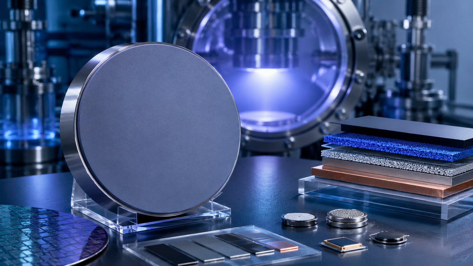
For physical vapor deposition projects, TFM supplies customizable Hafnium Oxide Sputtering Targets in different purities, dimensions, shapes, and backing plate configurations.
This guide compares magnetron sputtering and ALD to help researchers and engineers select an appropriate HfO₂ deposition method for their applications.
Why Is HfO₂ Used in Thin-Film Devices?
HfO₂ is particularly important as a high-k dielectric material. Its dielectric constant is substantially higher than that of conventional silicon dioxide, allowing a device to maintain the required capacitance while using a physically thicker insulating layer.
This can help reduce direct tunneling leakage in miniaturized semiconductor structures.
Depending on deposition conditions, film structure, doping, and post-deposition treatment, HfO₂ thin films can provide:
- A relatively high dielectric constant
- A wide electronic band gap
- Good thermal and chemical stability
- A high refractive index
- Good transparency over selected optical wavelength ranges
- Compatibility with semiconductor fabrication processes
- Potential ferroelectric behavior in selected doped or stabilized phases
- Resistance to demanding thermal and chemical environments
These properties support the use of HfO₂ in:
- MOSFET gate dielectric layers
- Metal-insulator-metal capacitors
- Thin-film transistors
- Resistive switching devices
- Ferroelectric memory structures
- Optical interference coatings
- High-power laser optics
- Protective and corrosion-resistant coatings
- Sensors and experimental electronic devices
The electrical and optical properties of deposited HfO₂ are not fixed values. They depend on film thickness, crystal phase, defect concentration, deposition temperature, substrate condition, and thermal treatment.
Research on ALD-prepared high-k HfO₂ thin films has demonstrated that film thickness, crystallinity, grain size, and annealing conditions can substantially affect dielectric behavior and breakdown performance.
How Magnetron Sputtering Deposits HfO₂ Films
Magnetron sputtering is a physical vapor deposition process performed inside a vacuum chamber.
A plasma is generated using a working gas, typically argon. Positively charged argon ions bombard the source target and transfer momentum to atoms or molecular species at the target surface. The ejected material travels through the vacuum chamber and condenses on the substrate.
There are two principal sputtering routes for depositing HfO₂.
Direct Sputtering from an HfO₂ Ceramic Target
In direct sputtering, a sintered HfO₂ ceramic target is used as the source material.
Because fully oxidized hafnium oxide is electrically insulating, radio-frequency magnetron sputtering is generally used instead of conventional direct-current sputtering. RF power helps prevent charge accumulation on the target surface and enables a stable plasma to be maintained.
A controlled amount of oxygen may be added to the argon process gas to compensate for oxygen loss during deposition or to improve film stoichiometry.
The main process variables include:
- RF power and power density
- Argon pressure
- Oxygen partial pressure
- Substrate temperature
- Substrate bias
- Target-to-substrate distance
- Deposition time
- Substrate rotation
- Post-deposition annealing
Direct sputtering from an oxide target can simplify composition development because oxygen is already present in the target. Nevertheless, target density, ceramic uniformity, surface condition, thermal conductivity, and plasma stability remain important.
Studies of magnetron-sputtered HfO₂ optical coatings have shown that sputtering power can influence film microstructure, crystal phase, and crystallite size. Power should therefore be optimized together with gas flow, chamber pressure, and substrate conditions.
Reactive Sputtering from a Hafnium Metal Target
HfO₂ can also be deposited by sputtering a metallic Hafnium Sputtering Target in a controlled argon-oxygen atmosphere.
Hafnium atoms are ejected from the conductive metal target and react with oxygen during transport through the plasma or after reaching the substrate.
Reactive sputtering provides flexibility for adjusting oxygen content and may offer a higher deposition rate when the target operates in metallic mode. However, oxygen flow must be carefully controlled.
Excessive oxygen can oxidize the target surface, causing target poisoning. This may lead to:
- Reduced deposition rate
- Changes in discharge voltage
- Plasma instability
- Process hysteresis
- Composition variation
- Arcing or particle generation
A ceramic HfO₂ target may therefore be preferred when a direct oxide source and simplified composition control are required. A metallic hafnium target may be selected when reactive-process flexibility, target conductivity, or access to pulsed-DC power is more important.
How Atomic Layer Deposition Produces HfO₂ Films
Atomic layer deposition is a vapor-phase chemical deposition method based on sequential and self-limiting surface reactions.
During a typical HfO₂ ALD cycle, the substrate is first exposed to a volatile hafnium-containing precursor. The precursor reacts with available surface sites until the reaction becomes saturated.
Excess precursor and gaseous reaction products are then removed with an inert purge gas.
The surface is subsequently exposed to an oxidizing co-reactant, such as:
- Water vapor
- Ozone
- Oxygen plasma
- Another oxygen-containing reactant
The oxidant converts the adsorbed hafnium-containing layer into hafnium oxide and regenerates reactive surface groups for the next cycle.
A simplified ALD sequence is:
- Hafnium precursor exposure
- Inert-gas purge
- Oxidant exposure
- Second purge
- Repetition until the required film thickness is reached
Because each half-reaction is designed to stop after available surface sites have reacted, the amount of material deposited during each cycle can be closely controlled.
Film thickness is therefore primarily adjusted by changing the number of ALD cycles.
The resulting film properties still depend on:
- Hafnium precursor chemistry
- Oxidant selection
- Deposition temperature
- Pulse duration
- Purge duration
- Reactor pressure
- Substrate surface chemistry
- Plasma conditions, when PEALD is used
- Post-deposition annealing
Magnetron Sputtering vs ALD: Main Differences
| Comparison Factor | Magnetron Sputtering | Atomic Layer Deposition |
|---|---|---|
| Deposition principle | Physical ejection from a solid target | Sequential chemical surface reactions |
| Source material | HfO₂ ceramic target or metallic Hf target | Volatile hafnium precursor and oxidant |
| Typical power mode | RF for ceramic HfO₂; DC or pulsed DC for metallic Hf | Thermal or plasma-enhanced reaction |
| Thickness control | Deposition rate and processing time | Number of ALD cycles |
| Deposition speed | Generally higher for moderate or thick films | Generally slower due to dosing and purging |
| Conformality | Best on planar or moderately structured surfaces | Excellent on complex 3D structures |
| Directionality | More line-of-sight dependent | Surface-reaction driven |
| Large-area coating | Well suited to scalable PVD systems | Possible, but cycle time may limit throughput |
| Film thickness range | Nanometer films through relatively thick coatings | Particularly effective for ultrathin layers |
| Primary consumable | Sputtering target and process gases | Chemical precursor, oxidant, and purge gas |
| Main strength | Throughput, scalability, and solid-source deposition | Thickness precision and conformality |
| Common challenge | Plasma damage, arcing, particles, and line-of-sight coverage | Slow growth, precursor cost, and residual impurities |
Film Thickness Control and Deposition Rate
One of the clearest differences between magnetron sputtering and ALD is the balance between deposition speed and thickness precision.
Magnetron Sputtering
Magnetron sputtering can deposit HfO₂ at a practical rate for films ranging from several nanometers to hundreds of nanometers or more, depending on the system and application.
Film thickness is controlled through:
- Deposition-rate calibration
- RF or DC power
- Working pressure
- Gas-flow ratio
- Substrate motion
- Total deposition time
With stable operating conditions and suitable thickness monitoring, sputtering can provide good repeatability across multiple runs.
Its higher practical deposition rate makes it attractive for:
- Optical coatings
- Protective films
- Planar capacitor structures
- Research wafers
- Large substrates
- Multilayer film systems
Atomic Layer Deposition
ALD adds only a small amount of material during each reaction cycle.
This makes it exceptionally suitable for ultrathin films where a thickness difference of one or two nanometers can significantly affect device performance.
The trade-off is throughput. Each ALD cycle requires separate precursor exposure and purge stages. Hundreds or thousands of cycles may be needed to build a thicker film.
As a practical selection guideline:
- Choose ALD when ultrathin-film precision is essential.
- Choose magnetron sputtering when higher throughput or greater film thickness is required.
Conformality on Complex Substrates
ALD provides a major advantage when HfO₂ must coat:
- Deep trenches
- Narrow vias
- Nanopores
- Three-dimensional semiconductor structures
- Nanoparticles
- Porous materials
- High-aspect-ratio surfaces
Because ALD is driven by surface reactions rather than predominantly directional particle transport, precursor molecules can reach surfaces that are not directly facing the source.
Sufficient precursor exposure and purge time are still required, particularly when coating deep or highly porous structures.
Magnetron sputtering is more directional. Substrate rotation, increased process pressure, off-axis deposition, specialized fixtures, or collimated source designs can improve coverage, but deeply recessed features may still receive less material than exposed surfaces.
For planar wafers, glass substrates, metal coupons, or moderately shaped components, sputtering may provide sufficient uniformity.
For advanced three-dimensional device geometries, ALD normally offers more dependable conformal coverage.
Film Density, Surface Roughness, and Defect Control
Both magnetron sputtering and ALD can produce dense, smooth HfO₂ films when properly optimized. Neither process automatically guarantees a defect-free coating.
Sputtered HfO₂ Films
The quality of a sputtered film is affected by:
- Target purity
- Target density
- RF power
- Working pressure
- Oxygen flow
- Substrate temperature
- Substrate bias
- Deposition rate
- Chamber cleanliness
- Target conditioning
- Annealing conditions
Energetic plasma species can promote dense film growth. However, excessive ion bombardment can introduce:
- Residual stress
- Interfacial damage
- Resputtering
- Surface defects
- Substrate heating
- Changes in film stoichiometry
Published research on the surface morphology and optical properties of magnetron-sputtered HfO₂ films describes sputtering advantages such as controllable thickness, good adhesion, film uniformity, and process flexibility.
ALD HfO₂ Films
ALD generally provides excellent roughness control and uniformity for ultrathin coatings.
Potential ALD-related defects or impurities can arise from:
- Incomplete precursor reactions
- Insufficient purge time
- Residual precursor ligands
- Carbon or chlorine contamination
- Hydroxyl groups
- Nucleation delay
- Non-ideal deposition temperature
- Incomplete oxidation
ALD film quality should therefore be evaluated through composition, density, leakage-current, breakdown, and interface measurements rather than thickness uniformity alone.
Stoichiometry and Oxygen Vacancy Control
Oxygen vacancies strongly influence the electrical and optical behavior of HfO₂ films.
They may affect:
- Leakage current
- Charge trapping
- Dielectric loss
- Refractive index
- Optical absorption
- Breakdown strength
- Resistive switching
- Ferroelectric phase formation
Oxygen Control During Sputtering
During direct HfO₂ sputtering, oxygen deficiency may occur because oxygen is preferentially removed from the target or growing film.
Introducing oxygen into the chamber can help restore stoichiometry. However, excessive oxygen may reduce deposition rate or alter plasma behavior.
Reactive sputtering from metallic hafnium requires even tighter oxygen-flow control because the target may transition between:
- Metallic mode
- Partially oxidized mode
- Fully poisoned oxide mode
The stable process window must be identified experimentally for each chamber and cathode configuration.
Oxygen Control During ALD
In ALD, stoichiometry is influenced by the interaction between the hafnium precursor and oxidizing co-reactant.
Water, ozone, and oxygen plasma can produce differences in:
- Oxygen-vacancy concentration
- Residual impurity content
- Film density
- Crystal structure
- Interface passivation
Research comparing different ALD co-reactants for HfOₓ deposition has shown that oxidant selection can affect composition, stoichiometry, crystallinity, and surface passivation.
Post-deposition annealing in oxygen, nitrogen, forming gas, or another controlled atmosphere may be used to modify defect concentration and film structure.
Interface Quality and Substrate Damage
ALD is widely selected for semiconductor gate stacks because it can deposit ultrathin HfO₂ layers with precise thickness control and relatively gentle thermal surface reactions.
However, ALD nucleation depends strongly on substrate chemistry.
Chemically inert surfaces may not contain enough reactive sites for immediate and uniform precursor adsorption. Such surfaces may require:
- Surface functionalization
- Plasma activation
- Ozone pretreatment
- A seed layer
- Enhanced precursor exposure
- Alternative precursor chemistry
Research into HfO₂ ALD nucleation and dielectric growth has shown that surface chemistry and oxygen-containing surface sites can substantially influence initial film formation.
Magnetron sputtering does not rely on the same self-limiting adsorption mechanism and can deposit onto a broad range of substrates.
However, the plasma environment introduces a different concern. Energetic ions, reflected particles, ultraviolet radiation, and fast neutral species may damage sensitive substrates or interfaces.
Potential mitigation methods include:
- Lower sputtering power
- Higher working pressure
- Increased target-to-substrate distance
- Off-axis geometry
- Substrate shielding
- Remote plasma arrangements
- Reduced substrate bias
The process choice should therefore consider whether poor chemical nucleation or plasma-induced damage presents the greater risk.
Crystallinity and Post-Deposition Annealing
As-deposited HfO₂ films may be amorphous or nanocrystalline depending on process temperature, thickness, energetic bombardment, and substrate properties.
Post-deposition annealing may be used to:
- Increase film density
- Modify crystal phase
- Reduce selected defects
- Change oxygen-vacancy concentration
- Improve dielectric performance
- Stabilize ferroelectric or related phases
- Adjust residual stress
However, annealing can also cause:
- Grain growth
- Increased surface roughness
- Interfacial reactions
- Element diffusion
- Film cracking
- Changes in leakage behavior
The annealing atmosphere and thermal budget should therefore be optimized for the substrate and device structure.
For semiconductor applications, interface stability may be more important than maximizing crystallinity. For optical coatings, low absorption, controlled refractive index, and mechanical stability may receive greater priority.
Large-Area Uniformity and Production Scalability
Magnetron sputtering is widely used for large-area coating because cathodes, substrate motion, rotating fixtures, and in-line vacuum systems can be scaled for production.
Uniformity depends on:
- Target dimensions
- Erosion profile
- Magnetic-field design
- Gas distribution
- Cathode-to-substrate geometry
- Substrate rotation or translation
- Chamber pressure
With suitable source design, sputtering can coat multiple substrates or large planar surfaces at practical production rates.
ALD can also provide excellent uniformity across large batches when precursor distribution and reactor geometry are well designed. However, the sequential cycle structure may restrict throughput.
Precursor consumption and purge time may become significant for:
- Large chambers
- High-volume substrates
- Deep porous structures
- Thick coatings
For mass production of ultrathin semiconductor dielectrics, ALD can justify its complexity. For thicker optical or protective coatings over large planar areas, sputtering may offer more favorable production economics.
Equipment and Consumable Requirements
Magnetron Sputtering Equipment
An HfO₂ sputtering system generally requires:
- Vacuum chamber
- Pumping system
- RF power supply
- Matching network
- Gas-flow controllers
- Magnetron cathode
- Substrate holder
- Cooling system
- Suitable ceramic target assembly
The primary consumables are the sputtering target and process gases.
For a ceramic target, the buyer should consider:
- Purity
- Relative density
- Target dimensions
- Dimensional tolerance
- Surface finish
- Backing plate
- Bonding method
- Recommended power
- Cathode compatibility
ALD Equipment
An ALD system requires:
- Heated reactor
- Precursor storage and delivery
- Temperature-controlled gas lines
- Pulse valves
- Oxidant supply
- Purge-gas control
- Exhaust treatment
- Chemical safety controls
The process must operate within an appropriate ALD temperature window. At an excessively low temperature, precursor condensation or incomplete reactions may occur. At an excessively high temperature, the precursor may decompose rather than react through the desired self-limiting mechanism.
HfO₂ for Optical Thin Films
HfO₂ is widely studied as a high-refractive-index material for optical coating systems.
Potential applications include:
- High-reflection coatings
- Anti-reflection coatings
- Interference filters
- UV optical coatings
- Laser mirrors
- Protective optical films
- Multilayer dielectric stacks
Magnetron sputtering is often selected for planar optical components because it provides practical deposition rates, scalable substrate handling, and control over film density.
HfO₂ may be combined with a lower-refractive-index material such as Silicon Dioxide Sputtering Target material to produce alternating HfO₂/SiO₂ multilayers.
The contrast between the refractive indices of the two materials allows engineers to design wavelength-selective optical stacks.
Important process considerations include:
- Refractive index
- Optical absorption
- Film stress
- Thickness accuracy
- Interface roughness
- Laser damage resistance
- Environmental stability
When Should Magnetron Sputtering Be Selected?
Magnetron sputtering is generally a strong starting point when:
- The substrate is planar or moderately structured.
- Moderate or thick HfO₂ films are required.
- Higher deposition throughput is important.
- Large-area coating capability is needed.
- Existing PVD equipment is available.
- A solid source is preferred over chemical precursors.
- Multilayer optical coatings are being developed.
- Film density and energetic growth need to be adjusted.
- Flexible materials screening is required.
- Precursor handling should be avoided.
Typical sputtering applications include optical coatings, planar capacitors, sensor structures, protective films, research wafers, and general thin-film development.
When Should ALD Be Selected?
ALD is generally favored when:
- The HfO₂ film must be extremely thin.
- Atomic-scale thickness control is required.
- The substrate contains deep trenches or vias.
- Highly conformal coverage is essential.
- Wafer-scale thickness uniformity must be tightly controlled.
- The film forms part of an advanced semiconductor gate stack.
- Interface engineering is central to device performance.
- A precisely controlled nanolaminate is required.
- Three-dimensional nanoscale structures must be coated.
Typical ALD applications include gate dielectrics, three-dimensional memory structures, conformal passivation layers, nanoscale capacitors, and coatings on porous substrates.
Can Sputtering and ALD Be Used Together?
Magnetron sputtering and ALD do not always need to be treated as competing processes.
A hybrid deposition flow can combine their respective advantages.
For example:
- ALD can deposit an ultrathin conformal interface layer.
- Sputtering can build a thicker functional or optical layer.
- A sputtered electrode can be combined with an ALD dielectric.
- ALD HfO₂ can be integrated between sputtered conductive layers.
- A sputtered seed layer can improve subsequent film growth.
- ALD can passivate a sputtered coating.
Hybrid structures may also combine HfO₂ with SiO₂, Al₂O₃, ZrO₂, TiO₂, or conductive materials.
The deposition sequence should account for:
- Interface cleanliness
- Vacuum exposure
- Surface oxidation
- Thermal budget
- Residual stress
- Adhesion
- Electrical contact
- Optical interference
Practical Process Selection Table
| Project Requirement | Recommended Starting Method | Reason |
|---|---|---|
| Ultrathin gate dielectric | ALD | Precise cycle-controlled thickness |
| High-aspect-ratio structure | ALD | Superior conformality |
| Planar optical coating | Magnetron sputtering | Practical rate and scalable coating |
| HfO₂/SiO₂ multilayer | Magnetron sputtering | Efficient multilayer PVD processing |
| Thick HfO₂ functional layer | Magnetron sputtering | Higher practical deposition rate |
| Atomic-level thickness adjustment | ALD | Self-limiting surface reactions |
| Large planar substrate | Magnetron sputtering | Established large-area systems |
| Porous or complex substrate | ALD | Better internal surface coverage |
| Low precursor-handling preference | Magnetron sputtering | Uses a solid target source |
| Advanced semiconductor gate stack | ALD | Interface and thickness control |
| Flexible laboratory PVD research | Magnetron sputtering | Convenient process adjustment |
| Hybrid interface and bulk layer | ALD plus sputtering | Combines conformality and throughput |
This table should be treated as a starting point. Final selection depends on film thickness, substrate geometry, electrical or optical requirements, thermal budget, equipment availability, and production volume.
How to Select an HfO₂ Sputtering Target
For magnetron sputtering projects, target quality directly affects process stability and coating consistency.
A suitable HfO₂ target should provide:
- Uniform chemical composition
- Controlled impurity levels
- High and consistent density
- Stable plasma behavior
- Resistance to thermal cracking
- Controlled erosion
- Reliable backing plate bonding
- Accurate dimensions
TFM supplies Hafnium Oxide Sputtering Targets with available purities of 99.9%, 99.95%, and 99.99%. Standard and customized forms include discs, plates, column targets, step targets, and drawing-based geometries.
Typical HfO₂ Target Parameters
| Parameter | Typical Options | Importance |
|---|---|---|
| Material | Hafnium oxide, HfO₂ | Determines deposited oxide chemistry |
| Purity | 99.9%, 99.95%, 99.99% | Helps control unwanted contamination |
| Shape | Disc, plate, column, step, or custom | Must match the cathode design |
| Diameter or length | Standard or customized | Ensures system compatibility |
| Thickness | Based on cathode and service-life requirements | Influences mechanical strength and usable material |
| Density | High-density sintered ceramic preferred | Supports stable erosion and reduces particle risk |
| Backing plate | Copper, molybdenum, titanium, or customized | Provides support and heat transfer |
| Bonding | Indium, elastomer, or mechanical mounting | Influences thermal management |
| Surface finish | Ground or lapped as specified | Supports proper mounting and plasma stability |
| Documentation | CoA and dimensional inspection | Supports incoming quality verification |
Additional oxide and compound materials are available through TFM’s Sputtering Targets portfolio.
RFQ Checklist for HfO₂ Sputtering Targets
To receive an accurate technical review and quotation, buyers should provide:
- Material: HfO₂
- Required purity
- Target shape
- Diameter or rectangular dimensions
- Target thickness
- Dimensional tolerances
- Required density, when specified
- Surface-finish requirement
- Backing plate material
- Backing plate dimensions
- Bonding method
- Cathode or sputtering-system model
- Expected RF power
- Quantity
- Required documentation
- Delivery destination
A drawing is recommended for stepped targets, bonded assemblies, unusual edge profiles, or nonstandard geometries.
Frequently Asked Questions
Is ALD always better than sputtering for HfO₂?
No. ALD is generally better for ultrathin and highly conformal coatings. Magnetron sputtering can offer higher throughput and better economics for planar, large-area, or thicker films.
Can an HfO₂ ceramic target be sputtered using DC power?
Fully oxidized HfO₂ is electrically insulating, so RF sputtering is normally used. Metallic hafnium targets can be sputtered using DC or pulsed-DC power in a reactive oxygen atmosphere.
Is an Hf metal target or HfO₂ target better?
An HfO₂ target provides a direct oxide source and may simplify film-composition development. A metallic Hf target is conductive and offers reactive-process flexibility, but oxygen flow and target poisoning must be carefully managed.
Which method produces smoother HfO₂ films?
Both methods can produce smooth films. ALD generally offers excellent roughness and thickness uniformity for ultrathin coatings. Optimized sputtering can produce smooth, dense films for optical and electronic applications.
Which process is better for optical coatings?
Magnetron sputtering is often preferred for planar optical coatings because it supports practical deposition rates, multilayer production, and scalable substrate handling.
Does HfO₂ target density affect sputtering performance?
Yes. Target density can influence plasma stability, thermal behavior, particle generation, and erosion. A dense and uniform ceramic target is generally preferred.
Can ALD HfO₂ be deposited at low temperatures?
Low-temperature ALD processes are possible, but film density, residual ligands, impurity concentration, and electrical properties must be evaluated. Plasma-enhanced ALD may improve reactivity at reduced temperatures.
Is annealing always required after HfO₂ deposition?
No. Annealing depends on the required crystal phase, electrical behavior, optical properties, defect concentration, and substrate thermal budget.
Can TFM provide bonded HfO₂ targets?
Bonded configurations can be evaluated according to the target dimensions, backing plate, operating power, and sputtering system. Customers should provide a target drawing or cathode information when requesting a bonded assembly.
What information is most important when requesting a quotation?
The required purity, target dimensions, backing plate, bonding method, quantity, system model, and destination are the most important initial details.
Conclusion
Magnetron sputtering and atomic layer deposition are both effective methods for producing HfO₂ thin films, but they serve different engineering priorities.
ALD provides exceptional conformality, cycle-level thickness control, and strong suitability for ultrathin dielectrics and three-dimensional device structures.
Magnetron sputtering provides higher practical deposition rates, flexible use of solid target materials, and scalable coating of planar or large-area substrates.
For advanced gate dielectrics and high-aspect-ratio nanoscale devices, ALD is usually the preferred starting point. For optical coatings, thicker functional films, planar research samples, and production environments where throughput matters, magnetron sputtering is often more practical.
The final process should be selected according to:
- Required film thickness
- Substrate geometry
- Interface sensitivity
- Film stoichiometry
- Desired crystal structure
- Production throughput
- Equipment availability
- Process cost
- Electrical or optical performance
For physical vapor deposition projects, TFM supplies high-purity Hafnium Oxide Sputtering Targets in standard and customized dimensions.
Available options include ceramic discs, plates, stepped targets, custom geometries, and targets bonded to suitable backing plates. Customers may provide their target drawing, required purity, dimensions, backing plate, bonding method, system model, and expected operating power for review.
For detailed specifications, customization, or a quotation, please contact TFM at sales@thinfilmmaterials.com.