

Product Overview
Germanium targets are specified according to the intended film, purity, conductivity type, resistivity, cathode design, mounting method, and thermal conditions.
For custom targets, provide a drawing or current assembly photo whenever possible. This allows the target dimensions, keeper features, bonding, backing plate, and cathode compatibility to be reviewed before quotation.
Key Procurement Point: Purity, N/P type, dopant, resistivity, target geometry, bonding, backing plate, and system conditions should be confirmed together.
Available Germanium Target Configurations
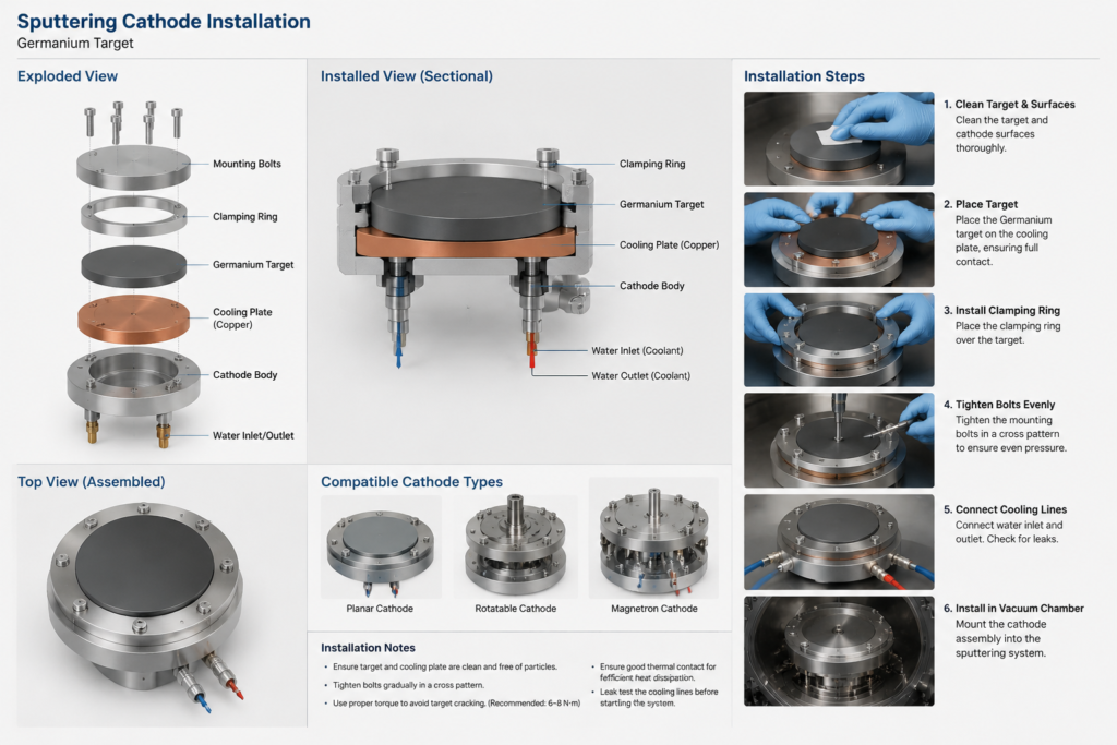
Planar Disc Targets
For standard circular sputtering cathodes. Confirm diameter, thickness, edge condition, purity, resistivity, and mounting method.
Rectangular & Segmented Targets
For inline, large-area, or custom deposition systems. Large or long Ge targets may require segmentation, bonding, and closer flatness review.
Step & Keeper Assemblies
For cathode-specific mounting. Provide step, keeper, hole pattern, flange, backing plate, and cooling details.
N-Type & P-Type Germanium
N-type, P-type, dopant, and resistivity requirements can be reviewed according to available germanium material and project requirements.
Indium-Bonded Targets
Bonding may be considered where additional support and improved heat transfer are required. Power and cooling must be reviewed with the complete assembly.
Custom Geometry
Made-to-drawing dimensions, edge features, mounting holes, keeper designs, backing assemblies, and other custom configurations can be reviewed for feasibility.
Key Specifications
| Specification | Available / Information to Provide |
| Material | Elemental Germanium, Ge |
| CAS Number | 7440-56-4 |
| Purity | 3N, 4N, 5N, and 6N options, subject to material availability and specification review |
| Electrical Specification | N-type, P-type, dopant, and required resistivity range |
| Shape | Disc, rectangular plate, step, segmented, keeper-mounted, or custom |
| Dimensions | Diameter or L × W, thickness, step, chamfer, flatness, and tolerance |
| Bonding | Unbonded or indium-bonded assembly |
| Backing Plate | Copper-backed or cathode-specific configuration |
| Surface and Edge | Ground, lapped, polished, cleaned, chamfered, or drawing-specific |
| Documentation | CoA, dimensional inspection, resistivity data, and agreed inspection records |
Germanium Sputtering Target – Key Specifications
Germanium Sputtering Target Applications
Infrared Optical Coatings
-1024x576.png)
Typical Use: Elemental Ge layers in infrared optical stacks, IR filters, thermal-imaging optics, and multilayer coating research.
Target Focus: Purity, surface condition, geometry, and repeatable material chemistry.
Semiconductor & Photodetector R&D

Typical Use: Ge semiconductor layers, Ge/Si interface studies, photodetectors, optoelectronic structures, and sensor devices.
Target Focus: Conductivity type, dopant, resistivity, purity, sputtering mode, and contamination limits.
Photovoltaic Thin-Film Research

Typical Use: Elemental Ge layers in photovoltaic interface studies, absorber-layer research, multilayer deposition, and experimental thin-film device development.
Target Focus: Purity, impurity control, film composition, target geometry, deposition-system compatibility, and process documentation.
How to Select a Germanium Sputtering Target
Selection Factor | What to Confirm | Why It Matters |
Purity | Required Ge purity and impurity limits | Higher purity may reduce unwanted impurities, but the highest grade is not necessary for every project. |
Conductivity Type and Resistivity | N-type, P-type, dopant, and Ω·cm range | These parameters may affect electrical behavior, plasma stability, and DC or RF selection. |
Sputtering Mode | DC, RF, pulsed DC, or system-specific process | DC may suit sufficiently conductive Ge; higher-resistivity material may require RF. |
Target Size and Geometry | Diameter or L × W, thickness, step, keeper, edge, and segment layout | Germanium is brittle, so large or complex targets require closer machining and handling review. |
Bonded or Unbonded | Direct clamping, indium bonding, or segmented assembly | Bonding may improve support and heat transfer, but the full assembly determines operating capability. |
Thermal Management | Backing plate, cooling, power, ramp rate, duty cycle, and run time | Heat removal, bond integrity, and thermal stress must be reviewed together. |
General Purity Guidance
- 3N–4N: Development work, process trials, and projects without strict impurity limits
- 5N: Semiconductor, infrared optical, photonic, and higher-purity thin-film research
- 6N: Impurity-sensitive projects requiring tighter trace-element control
These are general selection guidelines rather than universal application limits. Final purity should be based on impurity requirements, analytical methods, and film-performance objectives.
DC or RF Sputtering
Some conductive or controlled-resistivity Ge targets may be used with DC power. Higher-resistivity Ge may require RF sputtering or additional process review.
Magnetron describes the cathode configuration and should not be treated as a separate power mode beside DC and RF.
Power note: Published power guidance for one Ge target assembly should not be treated as a universal maximum. Actual allowable power depends on target dimensions, bonding, backing plate, cooling, thermal contact, orientation, ramp rate, and run conditions.
Germanium Target vs Similar Sputtering Target Materials
Target Material | Typical Deposited Film | Main Difference | When to Choose |
Elemental Ge film | Ge-specific semiconductor and infrared optical behavior | Choose when the required film is elemental germanium or a Ge-rich interface | |
Elemental Si film | Broader semiconductor use and generally lower cost | Choose when an Si film provides the required electrical, optical, or structural function | |
SiGe | Silicon-germanium alloy film | Adjustable Si/Ge composition | Choose when alloy ratio, strain, or band-structure tuning is part of the design |
Germanium oxide film | Oxide chemistry rather than elemental Ge | Choose when an oxygen-containing dielectric or optical layer is required |
Germanium vs SiGe
Choose Ge for elemental germanium films and SiGe when a controlled Si/Ge alloy ratio is required.
For R&D projects requiring adjustable film composition, dual- or multi-target co-sputtering may also be considered.
Germanium vs GeO₂
Choose Ge for elemental germanium films and GeO₂ when the required layer is a germanium oxide, dielectric, or oxygen-containing optical film.
Ge and GeO₂ are not direct substitutes because they produce films with different chemical compositions and functional properties.
Related Ge-Containing Alloy Target
For applications requiring a metallic Ge-containing alloy rather than pure Ge or germanium oxide, see the Aluminum Germanium Sputtering Target.
Design, Bonding, and Handling
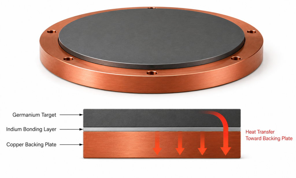
Edge Chipping
Germanium is brittle. Controlled edge geometry, even support, careful mounting, and protective packaging help reduce chipping and particle risk.
Heat Transfer
Bond quality, backing plate, cooling, thermal contact, and gradual power ramping affect thermal stress and assembly reliability.
Cathode Compatibility
Diameter, thickness, step, keeper, mounting holes, and cooling-well geometry should match the sputtering-source drawing.
| Option | When It May Be Considered | Main Review Point |
|---|---|---|
| Unbonded Target | Smaller targets, direct-clamping systems, or lower-power configurations | Uniform support, clamping pressure, and thermal contact |
| Indium-Bonded Target | Targets requiring improved support and heat transfer | Bond temperature, cooling, maximum power, and thermal cycling |
| Segmented Bonded Assembly | Long, rectangular, or large-area target designs | Segment layout, gap control, flatness, mounting, and cooling |
Custom Manufacturing, Inspection, and Documentation
Custom Manufacturing
We manufacture germanium sputtering targets in standard and custom configurations for laboratory and production cathode systems.
- Shapes: disc, rectangular, stepped, segmented, and custom
- Typical diameter range: Ø25.4–300 mm
- Typical thickness range: 1–20 mm
- Tolerances confirmed according to size, geometry, and drawing
- Copper backing plates and indium bonding available
Each configuration is reviewed for dimensional compatibility, mounting, thermal transfer, and sputtering stability.
Inspection Support
Germanium targets are inspected against the agreed material, dimensional, and drawing requirements before shipment.
- Diameter, length, width, and thickness inspection
- Flatness, parallelism, and surface-condition verification
- Chemical composition and impurity data, as specified
- Electrical resistivity verification, where required
- Bonding and assembly inspection, where applicable
- Compliance with agreed drawings and acceptance criteria
Additional inspection requirements can be included in the quotation and production plan.
Documentation and Packaging
Order-specific documentation and controlled packaging are available to support receiving inspection and quality-assurance procedures.
- Certificate of Analysis or material certificate
- Dimensional inspection report
- Resistivity test report, where specified
- Lot and batch traceability
- Bonding record for bonded assemblies
- Customer-specific document formats, subject to review
- Protected sputtering surface and moisture-resistant packaging
Documentation requirements should be confirmed before production.
RFQ Checklist
Minimum information: Purity, target dimensions, quantity, sputtering-system model, and drawing or current target photo.
- Required purity and impurity limits
- N-type, P-type, dopant, and resistivity
- Target shape and dimensions
- Quantity
- Bonded or unbonded configuration
- Backing-plate dimensions and material
- Cathode or sputtering-gun model
- DC / RF / other process mode
- Maximum power and cooling details
- Application and intended film
- Required inspection and documents
- Drawing, STEP, DWG, sketch, or current assembly photo
Frequently Asked Questions
It is used to deposit elemental Ge thin films by physical vapor deposition for infrared optical coatings, semiconductor layers, photodetectors, sensor structures, photovoltaic studies, and laboratory process development.
The required purity depends on the intended film and allowable impurity level. 3N–4N may suit general research, 5N is commonly reviewed for semiconductor and optical work, and 6N may be specified for impurity-sensitive projects.
Bonding should be considered for larger, thinner, stepped, rectangular, or higher-power targets because it may improve mechanical support and heat transfer.
Related Thin-Film Materials and Applications
Request a Germanium Target Quote
Send your required purity, conductivity type, resistivity, target dimensions, quantity, backing plate, system model, operating power, and drawing for technical review.