
Introduction
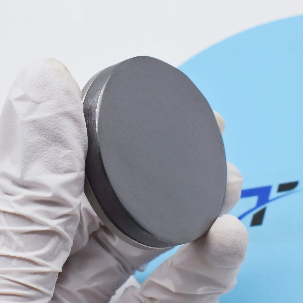
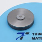
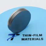
The Selenium Sputtering Target (Se) is a high-purity elemental target used in thin film deposition for semiconductor, photovoltaic, and optoelectronic applications. Selenium plays a crucial role in many compound semiconductor systems, particularly in chalcogenide materials and thin-film solar technologies. When deposited as a thin film through magnetron sputtering or other physical vapor deposition (PVD) processes, selenium contributes to the formation of functional materials with unique optical and electronic properties.
Selenium-based thin films are widely used in CIGS solar cells, photodetectors, phase-change materials, and semiconductor research, making selenium sputtering targets an important component in modern materials engineering and energy technologies.
Detailed Description
Selenium sputtering targets are typically manufactured from high-purity selenium through controlled casting, pressing, or sintering processes to achieve a dense and uniform target structure. High purity is essential because even small amounts of impurities can significantly affect the electrical and optical properties of selenium-containing thin films.
Selenium belongs to the chalcogen group of elements and exhibits semiconducting properties with strong photoelectric sensitivity. In thin film deposition systems, selenium is often used either as a standalone film or as a precursor material for compound semiconductor layers.
One of the most important applications of selenium sputtering targets is in the production of copper indium gallium selenide (CIGS) absorber layers used in high-efficiency thin-film solar cells. Selenium also plays a role in the synthesis of other compound materials such as zinc selenide (ZnSe), cadmium selenide (CdSe), and other chalcogenide semiconductors.
High-density selenium targets help ensure stable sputtering rates and uniform film composition during deposition. For improved mechanical stability and thermal management, selenium sputtering targets may also be supplied as bonded targets with copper backing plates, typically using indium bonding.
Applications
Selenium sputtering targets are used in several advanced technology sectors:
Thin film solar cells, particularly CIGS photovoltaic absorber layers
Compound semiconductor deposition for optoelectronic devices
Infrared and photodetector materials
Chalcogenide semiconductor research and thin film electronics
Optical coatings requiring specific absorption properties
Advanced materials development in research laboratories
Technical Parameters
| Parameter | Typical Value / Range | Importance |
|---|---|---|
| Purity | 99.9% – 99.999% | High purity ensures stable electronic and optical film properties |
| Chemical Symbol | Se | Determines elemental composition of thin films |
| Diameter | 25 – 300 mm (custom) | Compatible with standard sputtering systems |
| Thickness | 3 – 6 mm | Influences sputtering stability and target lifetime |
| Density | ≥ 95% theoretical density | Ensures uniform sputtering and film growth |
| Bonding | Copper backing plate / Indium bonded | Improves thermal stability during deposition |
Comparison with Related Materials
| Material | Key Advantage | Typical Application |
|---|---|---|
| Selenium (Se) | Strong photoelectric response and semiconductor properties | Solar cells and photodetectors |
| Tellurium (Te) | Excellent thermoelectric and semiconductor properties | Thermoelectric materials and detectors |
| Sulfur (S) | Important chalcogen element for compound semiconductors | Semiconductor synthesis and coatings |
FAQ
| Question | Answer |
|---|---|
| What sputtering methods are suitable for selenium targets? | Selenium sputtering targets can be used in RF or DC magnetron sputtering systems depending on system configuration. |
| Can selenium targets be customized? | Yes. Diameter, thickness, and bonding options can be customized to match different sputtering systems. |
| Are bonded sputtering targets available? | Yes. Selenium targets can be bonded to copper backing plates using indium bonding for improved thermal management. |
| What purity levels are typically available? | Standard purities range from 99.9% up to 99.999% depending on application requirements. |
| What substrates can selenium films be deposited on? | Selenium films can be deposited on glass, silicon wafers, metal substrates, and other semiconductor materials. |
Packaging
Our Selenium Sputtering Target (Se) products are meticulously tagged and labeled externally to ensure efficient identification and maintain strict quality control standards. Each target is packaged in vacuum-sealed bags with protective foam and export-grade cartons or wooden crates to prevent contamination, oxidation, and mechanical damage during storage and transportation.
Conclusion
The Selenium Sputtering Target (Se) is an essential material for depositing semiconductor and chalcogenide thin films used in solar energy technologies, photodetectors, and advanced optoelectronic devices. Its unique photoelectric and semiconducting properties make it highly valuable for both industrial manufacturing and research applications.
With high-purity materials, customizable dimensions, and stable sputtering performance, selenium sputtering targets support a wide range of modern thin film technologies.
For detailed specifications and a quotation, please contact us at sales@thinfilmmaterials.com.


Reviews
There are no reviews yet.