
Tin Sputtering Target Description
T
Introduction
Tin Sputtering Targets are essential deposition materials for producing functional thin films used in electronics, optics, energy devices, and surface engineering. Owing to tin’s excellent electrical conductivity, low melting point, and compatibility with alloying systems, high-purity tin targets are widely applied in both research and industrial Physical Vapor Deposition (PVD) processes.
Detailed Description
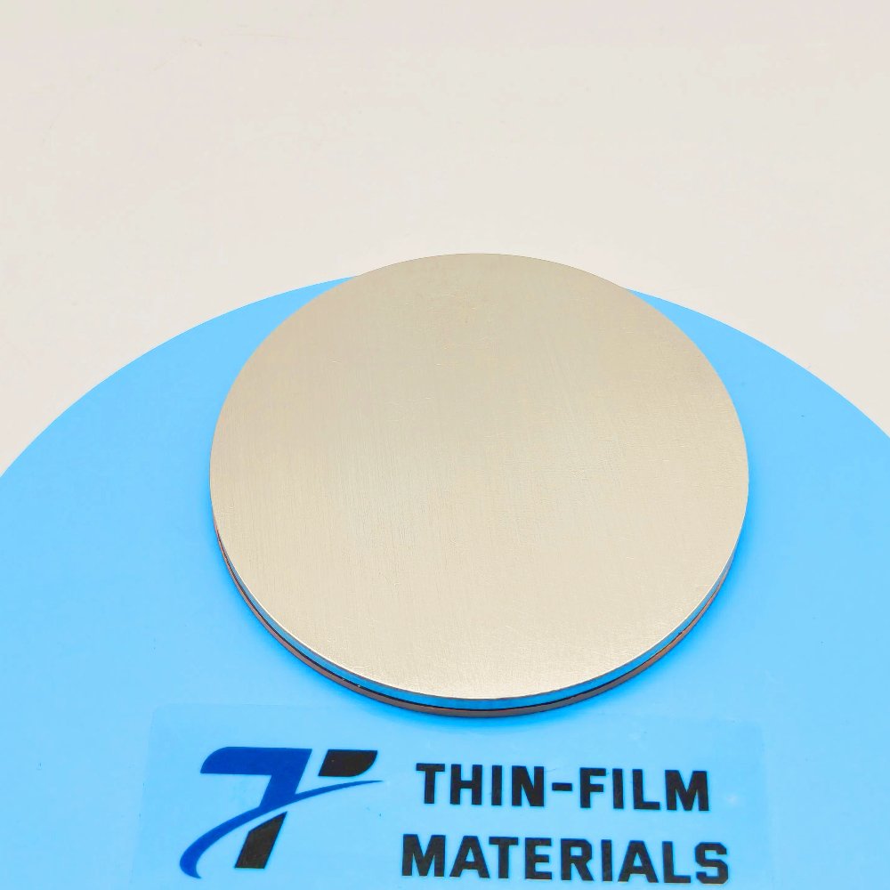
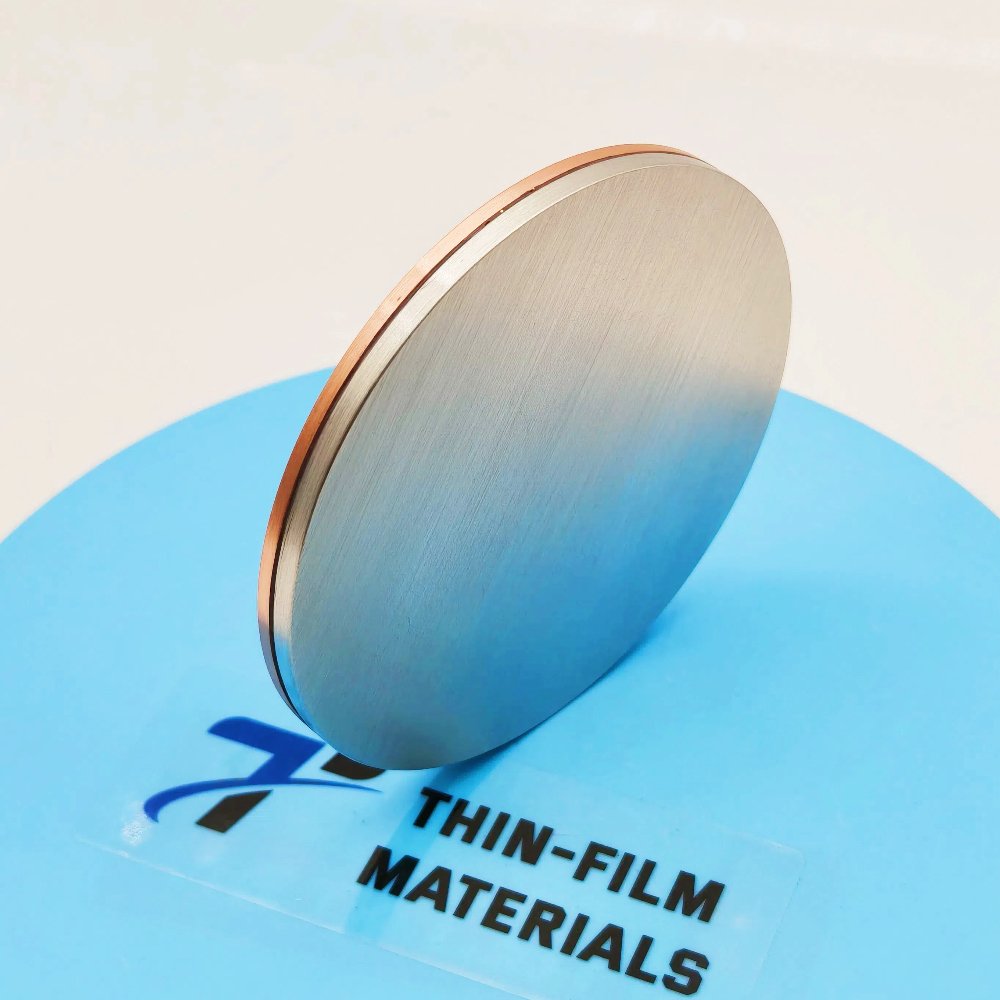
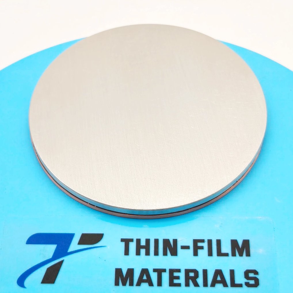
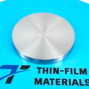
Tin sputtering targets are manufactured from refined, high-purity tin using controlled melting and forming processes to ensure uniform composition and consistent density. Because tin is a relatively soft metal with a low melting point, careful control of target flatness, surface finish, and bonding quality is critical to achieve stable sputtering performance and long target life.
Targets can be supplied unbonded for small diameters or low-power applications, or bonded to copper backing plates to improve thermal conductivity and mechanical stability during higher-power magnetron sputtering. Proper bonding helps prevent warping, localized overheating, and premature target failure.
Tin targets are compatible with DC magnetron sputtering and are also commonly used as alloy components (e.g., ITO, SnO₂-based films, or metal alloy layers) where precise compositional control is required.
Applications
Transparent conductive and oxide thin films
Semiconductor and microelectronic coatings
Solderable and conductive layers
Decorative and corrosion-resistant coatings
Thin film research and materials development
Technical Parameters
| Parameter | Typical Value / Range | Importance |
|---|---|---|
| Material | Tin (Sn) | Conductive functional metal |
| Purity | 99.9% – 99.999% | Impurity control affects film quality |
| Form | Disc / Plate (bonded or unbonded) | Fits sputtering systems |
| Diameter | 25 – 300 mm (custom) | Matches magnetron cathodes |
| Thickness | 3 – 6 mm (typical) | Influences target lifetime |
| Backing Plate | Copper (optional) | Improves heat dissipation |
Comparison with Related Materials
| Material | Key Advantage | Typical Application |
|---|---|---|
| Tin (Sn) | Low melting point, good conductivity | Electronics & coatings |
| Indium (In) | Soft metal, oxide applications | Transparent electrodes |
| Zinc (Zn) | Cost-effective | Protective & functional films |
FAQ
| Question | Answer |
|---|---|
| Can tin sputtering targets be customized? | Yes, size, purity, thickness, and bonding can be tailored. |
| Are bonded tin targets recommended? | Yes, copper-backed targets are preferred for higher power sputtering. |
| Is DC sputtering suitable for tin? | Yes, tin is commonly used with DC magnetron sputtering. |
| Can large-diameter targets be supplied? | Yes, targets up to 300 mm or larger can be produced on request. |
| Is a Certificate of Analysis available? | Yes, CoA is available upon request. |
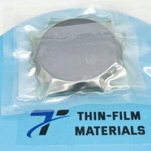
Packaging
Our Tin Sputtering Targets are cleaned for vacuum service, individually labeled, and vacuum-sealed to prevent oxidation and contamination. Shock-absorbing materials and export-grade cartons or wooden crates ensure safe transportation and storage.
Conclusion
Tin Sputtering Targets deliver stable sputtering behavior, high purity, and excellent process compatibility for a wide range of thin film applications. With flexible customization options and consistent quality control, they are a reliable choice for electronic, optical, and research-driven PVD processes.
For detailed specifications and a quotation, please contact us at sales@thinfilmmaterials.com.

Reviews
There are no reviews yet.