Introduction
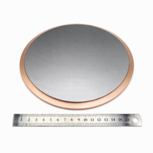
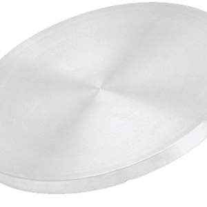
The ST0066 Aluminum Silicon Copper Sputtering Target (Al/Si/Cu) is a widely adopted alloy target engineered for advanced thin-film deposition processes. By combining aluminum with carefully controlled amounts of silicon and copper, this target delivers a balanced solution for applications that demand reliable electrical performance, strong adhesion, and long-term process stability. It is especially valued in semiconductor and microelectronics manufacturing, where consistent film properties and compatibility with large-scale sputtering systems are critical.
Detailed Description
Aluminum Silicon Copper sputtering targets are designed to address the limitations of pure aluminum films, such as poor electromigration resistance and mechanical instability under high current density. The addition of silicon helps suppress hillock formation and improves film smoothness, while copper enhances electrical conductivity and electromigration resistance.
ST0066 Al/Si/Cu targets are produced using high-purity raw materials and advanced melting and forming processes to ensure uniform composition and dense microstructure. This compositional homogeneity translates directly into stable sputtering behavior, predictable deposition rates, and reduced particle generation during operation.
The targets are available in various shapes and dimensions, including round, rectangular, and custom designs, with optional bonding to copper or titanium backing plates. Proper bonding improves thermal conductivity and mechanical stability, allowing the target to withstand higher power densities and extended sputtering cycles without warping or delamination.
Applications
Aluminum Silicon Copper Sputtering Targets are extensively used in industries requiring conductive and barrier thin films, including:
Semiconductor interconnect layers and metallization
Integrated circuits (ICs) and logic devices
Power devices and MEMS components
Flat panel displays and advanced packaging
Functional and protective coatings in electronics
These applications benefit from the alloy’s excellent balance of conductivity, adhesion, and reliability.
Technical Parameters
| Parameter | Typical Value / Range | Importance |
|---|---|---|
| Composition | Al / Si / Cu (custom ratios available) | Determines electrical and mechanical film properties |
| Purity | 99.9% – 99.99% | Reduces impurities and improves film consistency |
| Diameter / Size | 25 – 300 mm (custom available) | Compatible with different sputtering systems |
| Thickness | 3 – 6 mm (custom available) | Influences sputtering rate and target life |
| Bonding | Copper or Titanium backing plate | Enhances heat dissipation and stability |
| Surface Finish | Fine-machined, low roughness | Ensures uniform plasma interaction |
Comparison with Related Materials
| Material | Key Advantage | Typical Application |
|---|---|---|
| Aluminum Silicon Copper (Al/Si/Cu) | Improved electromigration resistance and stability | Semiconductor metallization |
| Aluminum (Al) | Simple composition, low cost | General conductive coatings |
| Aluminum Copper (Al/Cu) | Higher conductivity than pure Al | Power electronics |
| Aluminum Silicon (Al/Si) | Reduced hillock formation | IC barrier layers |
FAQ
| Question | Answer |
|---|---|
| Can the Al/Si/Cu ratio be customized? | Yes, compositions can be tailored to specific process requirements. |
| Is bonding to a backing plate necessary? | Bonding is recommended for better thermal management and longer target life. |
| What sputtering methods are compatible? | DC and RF magnetron sputtering systems. |
| How is target quality ensured? | Each target undergoes strict dimensional, compositional, and visual inspection. |
Packaging
Our ST0066 Aluminum Silicon Copper Sputtering Targets are carefully tagged and labeled for accurate identification and traceability. Each target is vacuum-sealed and protected with cushioning materials to prevent contamination or mechanical damage during storage and transportation. Export-grade cartons or wooden crates are used to ensure safe global delivery.
Conclusion
The ST0066 Aluminum Silicon Copper Sputtering Target (Al/Si/Cu) offers a proven combination of performance, reliability, and customization for demanding thin-film deposition applications. With controlled composition, excellent sputtering stability, and flexible sizing options, it is a dependable choice for semiconductor and advanced electronics manufacturing.
For detailed specifications and a quotation, please contact us at sales@thinfilmmaterials.com.


Reviews
There are no reviews yet.