
Introduction
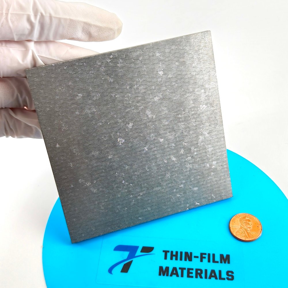
The Antimony Indium Tin Sputtering Target, SbInSn target, is a multi-component alloy target designed for advanced thin film deposition. By combining the semiconducting properties of indium, the conductivity of tin, and the modifying characteristics of antimony, this material enables the production of films with tailored electrical, optical, and structural performance. It is particularly attractive for next-generation optoelectronic devices, permanent memory devices, transparent conductive coatings, and research in compound semiconductors.
Detailed Description
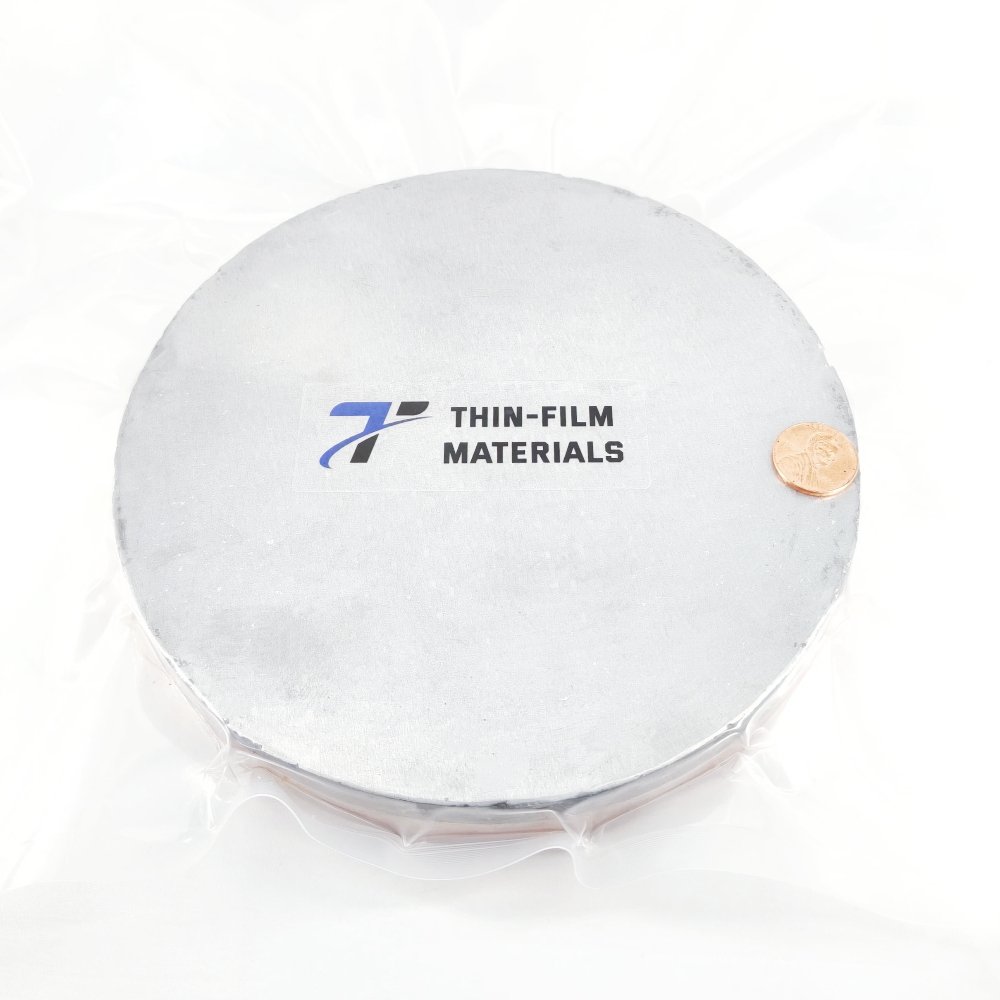
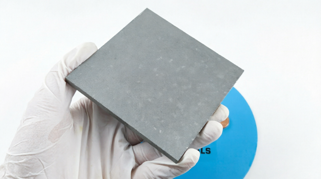
Antimony Indium Tin sputtering targets are manufactured through powder metallurgy and vacuum sintering, resulting in a dense, homogeneous target that delivers stable sputtering rates and uniform thin film composition.
Key features include:
High Purity (≥99.9%) – ensures low contamination and reproducible film properties.
Optimized Alloy Composition – Sb, In, and Sn can be tuned in different atomic ratios depending on customer requirements.
Stable Microstructure – minimizes cracking and enables long target life.
Custom Bonding Options – available with Indium or Elastomer bonding to copper backing plates for high-power sputtering systems.
These properties allow precise control of thin film characteristics, especially in applications where transparency, conductivity, and thermal stability must be balanced.
Applications
Antimony Indium Tin Sputtering Targets are widely used in:
Transparent Conductive Films (TCFs) – for displays, touch panels, and photovoltaics.
Semiconductor Devices – functional layers in electronic and optoelectronic components.
Thin Film Photovoltaics – coatings for solar cell electrodes and active layers.
Optical Coatings – films with tailored refractive and conductive properties.
R&D in Advanced Materials – studies on ternary/quaternary compound semiconductors.
Technical Parameters
| Parameter | Typical Value / Range | Importance |
|---|---|---|
| Purity | 99.9% – 99.99% | Ensures high-quality thin films |
| Composition | Sb/In/Sn (custom ratios available) | Tailors conductivity & transparency |
| Diameter | 25 – 200 mm | Fits standard sputtering systems |
| Thickness | 3 – 10 mm | Affects deposition stability |
| Bonding | Indium / Elastomer / Copper backing | Improves thermal management |
Comparison with Related Materials
| Material | Key Advantage | Typical Application |
|---|---|---|
| Antimony Indium Tin | Tunable optical/electrical properties | Transparent conductive films, semiconductors |
| Indium Tin Oxide (ITO) | High transparency & conductivity | Touchscreens, displays |
| Antimony Tin Oxide (ATO) | Cost-effective, stable coatings | Glass coatings, sensors |
FAQ
| Question | Answer |
|---|---|
| Can the Sb/In/Sn ratio be customized? | Yes, we provide standard and tailored compositions depending on application. |
| What industries use this target? | Electronics, photovoltaics, display technology, and optical coating industries. |
| How is it packaged? | Each target is vacuum-sealed, cushioned with protective foam, and shipped in export-grade cartons or wooden crates. |
| Is bonding available? | Yes, indium and elastomer bonding to copper plates are available for stability in high-power sputtering. |
| What deposition methods are suitable? | Primarily magnetron sputtering (DC or RF) in thin film production lines. |
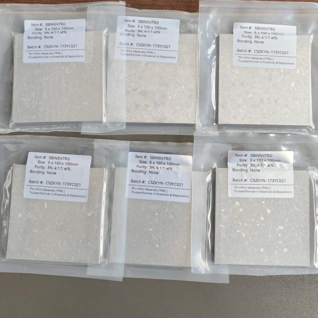
Packaging
Each Antimony Indium Tin Sputtering Target is vacuum-sealed in moisture-protective packaging and externally labeled for traceability. Targets are secured with foam inserts and shipped in sturdy export cartons or wooden crates, ensuring they arrive in perfect condition.
Conclusion
The Antimony Indium Tin Sputtering Target is a versatile alloy target material offering a balance of conductivity, transparency, and stability. With customizable composition, high purity, and reliable bonding options, it serves as a dependable choice for thin film applications in electronics, photovoltaics, and optics.
For detailed specifications and a quotation, please contact us at [sales@thinfilmmaterials.com].
1. What Is an SbInSn Sputtering Target?
An SbInSn sputtering target is a ternary alloy composed of antimony (Sb), indium (In), and tin (Sn), primarily used as a source material in Physical Vapor Deposition (PVD) processes to form functional thin films.
An Antimony Indium Tin (Sb/In/Sn) sputtering target is a ternary alloy composed of antimony (Sb), indium (In), and tin (Sn), widely used as a source material in Physical Vapor Deposition (PVD) processes for depositing functional thin films.
Unlike conventional single-metal targets, Sb/In/Sn is a phase-change alloy, capable of transitioning between amorphous and crystalline states under thermal stimulation. This property enables its use in applications where controlled optical response and structural transformation are required, particularly in optical storage and advanced electronic systems.
The most commonly used composition is:
Sb/In/Sn = 4:1:1 (atomic ratio)
This ratio offers an optimized balance of:
- Phase stability
- Optical contrast
- Deposition consistency
- Process compatibility
2. Why SbInSn Is Not an “Easy” Target to Manufacture
Although Sb/In/Sn may appear straightforward as an alloy system, it is one of the more difficult sputtering targets to manufacture reliably—especially when scaling beyond laboratory sizes.
From practical production experience, several critical challenges must be addressed:
Due to the different melting points and solidification behaviors of Sb, In, and Sn, maintaining uniform composition throughout the target requires precise process control. Poor control can result in localized compositional variation, directly affecting thin film performance.
Sb/In/Sn alloys have relatively low mechanical strength. During cooling, especially in larger diameters, internal stress can lead to cracking, reducing target yield and lifetime.
Machining and Surface Quality
Compared with refractory metals, Sb/In/Sn alloys are softer and more sensitive to deformation. Achieving a smooth, defect-free surface is essential to avoid arcing and ensure stable sputtering.
Scaling Limitations
While many suppliers can produce small targets (1–2 inches), manufacturing larger diameters requires significantly higher control over alloy uniformity and structural stability.
👉 Proven Capability:
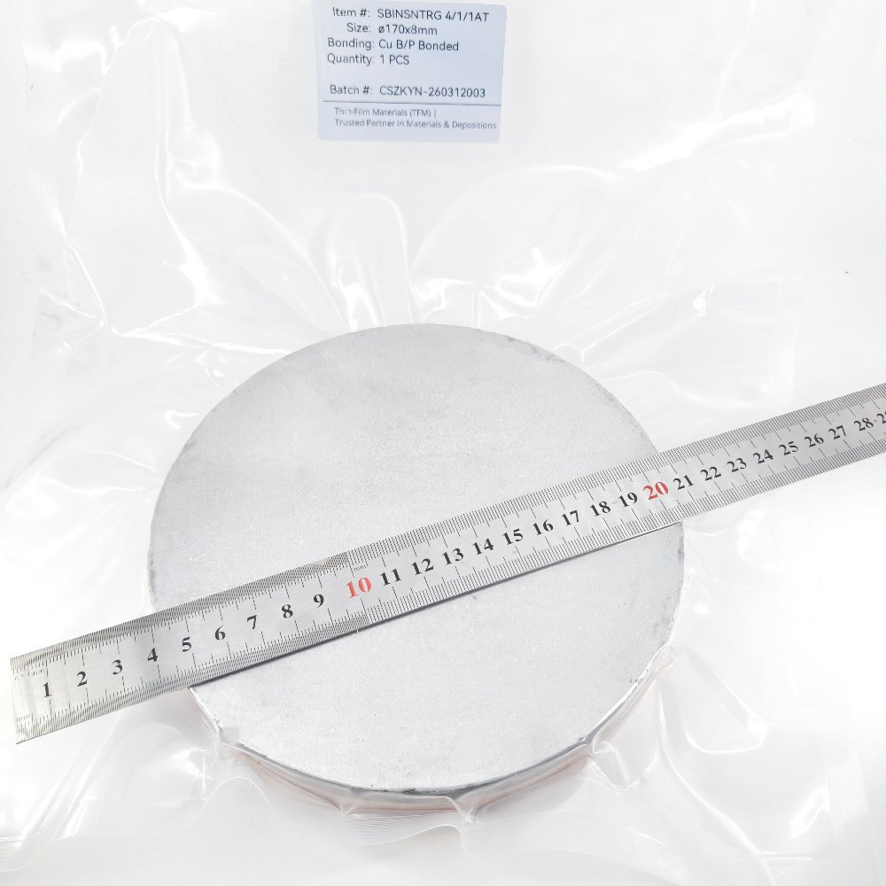
We have successfully produced Sb/In/Sn sputtering targets up to 170 mm in diameter, with consistent composition and repeatable performance across multiple production batches—meeting the requirements of both R&D and industrial-scale deposition.
3. How SbInSn Targets Work in Sputtering Processes
In a typical magnetron sputtering process:
- The Sb/In/Sn target is mounted inside a vacuum chamber
- Inert gas ions (typically argon) bombard the target surface
- Alloy atoms are ejected and deposited onto a substrate
- A functional thin film is formed
In many applications, the deposited film acts as a phase-change layer, where localized heating (such as laser input) induces structural transformation between amorphous and crystalline states.
From practical experience, sputtering performance is highly dependent on:
- Target density and consolidation – affects plasma stability
- Surface finish quality – reduces arcing and defects
- Composition uniformity – ensures consistent film properties
Even minor variations in these parameters can lead to significant differences in film performance, especially in precision applications.
4. Key Properties of SbInSn Thin Films
| Property | Relevance |
|---|---|
| Phase-change behavior | Enables permanent or controlled data storage |
| Optical contrast | Allows reliable readout in optical systems |
| Tunable crystallization | Adjusted via Sb/In/Sn ratio |
| Moderate melting point | Easier processing but higher risk of deformation |
| High purity availability (3N–5N) | Critical for thin film quality |
5. Real Application: Optical and Archival Data Storage
Although SbInSn is not widely discussed today, it still plays a role in specialized data storage technologies, particularly where long-term stability is required.
In one of our recent projects, we supplied Sb/In/Sn = 4:1:1 sputtering targets to a European company developing advanced data storage systems.
In that application:
The thin film required stable phase-change behavior
Uniform deposition over larger areas was critical
Batch consistency directly affected device performance
One thing we noticed during this project is that composition control becomes much more critical at larger target sizes, especially when uniform deposition is required.
This is where many standard suppliers struggle.
6. SbInSn vs ITO vs GeSbTe: Key Differences
| Material | Type | Typical Use |
|---|---|---|
| SbInSn | Phase-change alloy (write-once) | Archival optical storage |
| ITO (Indium Tin Oxide) | Transparent conductor | Displays, touch panels |
| GeSbTe (GST) | Phase-change alloy (rewritable) | Rewritable memory devices |
👉 In simple terms:
- Choose SbInSn for permanent storage
- Choose GST for rewritable systems
- Choose ITO for conductivity
7. Common Problems in SbInSn Sputtering (and How to Avoid Them)
From actual usage and feedback, several issues appear frequently:
Cracking During Operation
Cause: Thermal shock or internal stress
Solution: Gradual power ramping + proper cooling
Arcing
Cause: Surface defects or trapped gas
Solution: High-density target + surface inspection
Composition Drift in Film
Cause: Non-uniform erosion
Solution: Optimize sputtering parameters or consider geometry
Contamination
Cause: Handling or storage issues
Solution: Use clean gloves and vacuum packaging
8. How to Choose a Reliable SbInSn Target Supplier
Not all suppliers offering SbInSn targets have real production experience.
Here’s what we typically recommend evaluating:
1. Proven Manufacturing Experience
Ask if they have actually produced Sb/In/Sn 4:1:1 targets—not just listed them. Thin Film Materials has rich experience in producing such targets, our customer including companies developing next-generation ceramic-based data storage technologies.
2. Size Capability
If your process requires larger targets (>100 mm), confirm their actual maximum size capability. TFM has successful experience in producing ø170mm SbInSn Target.
3. Composition Control
Uniformity across the entire target is critical for film performance.
4. Batch Consistency
Especially important for production environments.
5. Technical Understanding
Suppliers familiar with sputtering behavior—not just material supply—are far more reliable.
9. Typical Specifications We Offer
- Composition: Sb/In/Sn = 4:1:1 (customizable)
- Purity: 99.9% – 99.999%
- Size: up to 170 mm diameter
- Forms: Planar / Rotary / Custom shapes
- Bonding: Available upon request
For detailed specifications, you can refer to our SbInSn sputtering target product page.
10. Why SbInSn Still Matters Today
SbInSn may not be a mainstream material today, but in certain applications, it remains highly relevant.
Based on what we’ve seen:
- It offers stable phase-change behavior
- It is suitable for long-term data storage
- It provides flexibility in composition tuning
More importantly, when manufactured correctly, it can deliver reliable and repeatable performance.
11. Need Sb/In/Sn 4:1:1 Targets for Your Application?
We supply high-quality SbInSn sputtering targets with:
- Custom compositions
- Large-size capability (up to 170 mm)
- Stable batch quality
- Experience in real data storage applications
If you are working on phase-change materials or optical storage systems, feel free to contact TFM with your requirements—we’re happy to discuss practical solutions.
You May Also Want to Know
1. What is an SbInSn sputtering target?
A ternary alloy target used to deposit thin films with phase-change properties.
2. What is Sb/In/Sn 4:1:1?
A standard atomic ratio offering balanced performance in optical storage applications.
3. What purity levels are available?
Typically from 3N (99.9%) up to 5N (99.999%).
4. Can SbInSn targets be made in large sizes?
Yes, but it requires advanced manufacturing control. Not all suppliers can do this reliably.
5. What is the main application of SbInSn?
Phase-change optical storage and related thin film applications.
6. What deposition methods are used?
Mainly magnetron sputtering and PVD processes.
7. What causes cracking in SbInSn targets?
Thermal stress during cooling or operation.
8. How should SbInSn targets be stored?
In clean, dry, vacuum-sealed or inert environments.
9. Is SbInSn still used today?
Yes, mainly in specialized and research applications.
10. Can composition be customized?
Yes, Sb/In/Sn ratios can be adjusted depending on application needs.
11. What experience does TFM have? / Case study
One of our recent projects involved supplying Sb/In/Sn = 4:1:1 targets to a leading European company specializing in next-generation data storage technologies.


Reviews
There are no reviews yet.