Introduction
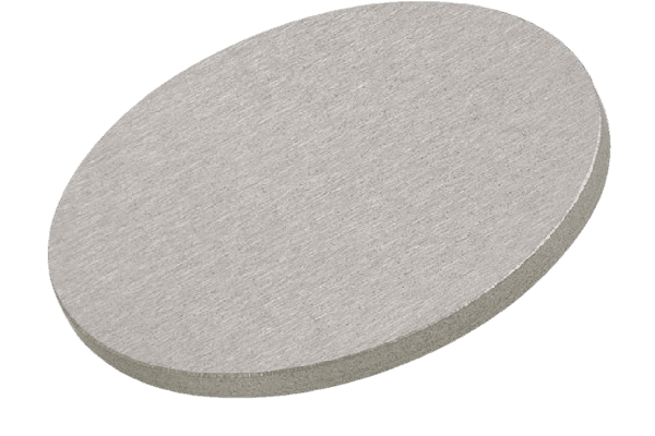
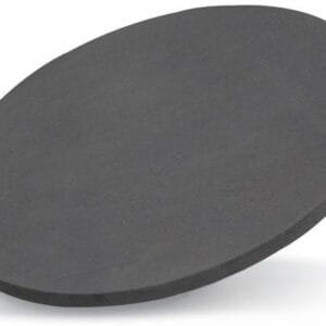
The Tin Arsenide Sputtering Target (SnAs) is a compound semiconductor target designed for the deposition of functional thin films in advanced electronic, optoelectronic, and research applications. Tin arsenide belongs to the family of metal arsenide materials that exhibit interesting electrical and structural properties, making them suitable for specialized semiconductor devices and experimental thin film systems.
Through physical vapor deposition (PVD) techniques such as magnetron sputtering, SnAs targets enable the formation of controlled thin films with precise stoichiometry. These films are studied and used in areas including semiconductor materials research, electronic device development, and emerging functional materials.
Detailed Description
Tin Arsenide sputtering targets are manufactured using high-purity tin and arsenic through controlled alloying and ceramic processing techniques such as vacuum melting, hot pressing, or sintering. These processes help ensure homogeneous composition, high density, and structural stability, which are essential for consistent sputtering performance.
SnAs is a compound material that combines the metallic properties of tin with the semiconducting characteristics of arsenic-based compounds. In thin film deposition, maintaining the correct Sn-to-As ratio is critical because it directly affects the electrical conductivity, crystal structure, and electronic properties of the resulting film.
High-density sputtering targets minimize particle generation during deposition and maintain stable sputtering rates. This is particularly important in semiconductor research environments where film uniformity and reproducibility are essential.
Depending on system requirements, SnAs sputtering targets can be produced as planar targets or bonded targets with copper backing plates, using indium bonding or diffusion bonding to improve heat dissipation and mechanical stability during high-power sputtering operations.
Applications
Tin Arsenide sputtering targets are used in several specialized technology and research fields:
Semiconductor thin film research involving arsenide-based materials
Electronic device development requiring compound semiconductor layers
Optoelectronic material studies focused on novel metal arsenide systems
Thin film electronics with controlled conductivity and structure
Advanced materials research in laboratories and academic institutions
Experimental coatings for electronic and sensing technologies
Technical Parameters
| Parameter | Typical Value / Range | Importance |
|---|---|---|
| Purity | 99.9% – 99.99% | Ensures stable semiconductor film properties |
| Chemical Formula | SnAs | Determines compound composition and electronic behavior |
| Diameter | 25 – 300 mm (custom) | Compatible with standard sputtering systems |
| Thickness | 3 – 6 mm | Influences sputtering efficiency and target lifetime |
| Density | ≥ 95% theoretical density | Improves deposition stability and film uniformity |
| Bonding | Copper backing plate / Indium bonded | Enhances heat dissipation during sputtering |
Comparison with Related Materials
| Material | Key Advantage | Typical Application |
|---|---|---|
| Tin Arsenide (SnAs) | Compound semiconductor properties with tunable conductivity | Experimental electronic and optoelectronic films |
| Gallium Arsenide (GaAs) | High electron mobility | High-speed electronics and optoelectronic devices |
| Indium Arsenide (InAs) | Narrow bandgap semiconductor | Infrared detectors and high-speed electronics |
FAQ
| Question | Answer |
|---|---|
| Can the SnAs sputtering target be customized? | Yes. Target diameter, thickness, and bonding configurations can be tailored to specific sputtering systems. |
| What deposition methods are suitable for SnAs targets? | SnAs sputtering targets are typically used in RF magnetron sputtering or other PVD techniques suitable for compound semiconductors. |
| Are bonded targets available? | Yes. Copper backing plates with indium bonding are commonly supplied for improved thermal management. |
| What purity levels are typically available? | Standard purity levels range from 99.9% to 99.99%, depending on application requirements. |
| What substrates can SnAs thin films be deposited on? | SnAs films can be deposited on silicon wafers, glass, ceramics, and other semiconductor substrates. |
Packaging
Our Tin Arsenide Sputtering Target (SnAs) products are meticulously tagged and labeled externally to ensure efficient identification and maintain strict quality control standards. Each target is packaged in vacuum-sealed bags with protective foam and export-grade cartons or wooden crates. These packaging methods prevent contamination, oxidation, and mechanical damage during storage and transportation.
Conclusion
The Tin Arsenide Sputtering Target (SnAs) provides a reliable material solution for depositing compound semiconductor thin films used in advanced electronics and research applications. Its controlled composition, high density, and stable sputtering behavior make it suitable for experimental semiconductor systems and optoelectronic materials development.
With customizable target configurations and high-purity materials, SnAs sputtering targets support consistent thin film deposition for both industrial and research environments.
For detailed specifications and a quotation, please contact us at sales@thinfilmmaterials.com.


Reviews
There are no reviews yet.