 MSDS File
Introduction
Indium Evaporation Materials (In) are high-purity metallic sources designed for thin film deposition via physical vapor deposition (PVD), including electron beam and thermal evaporation. Indium plays a critical role in semiconductor devices, transparent conductive films, infrared optics, and compound semiconductor fabrication.
Thanks to its low melting point, excellent wettability, and compatibility with oxide and III–V compound systems, indium is widely used in advanced electronics, optoelectronics, and display technologies.
Detailed Description
Indium (atomic number 49) is a soft, silvery post-transition metal with a low melting point of 156.6°C. This characteristic makes it particularly suitable for controlled evaporation processes at relatively low thermal loads.
Indium Evaporation Materials are refined to high purity levels to ensure:
Minimal contamination in deposited films
Stable and uniform evaporation rate
Reduced particle generation
Excellent film adhesion and electrical performance
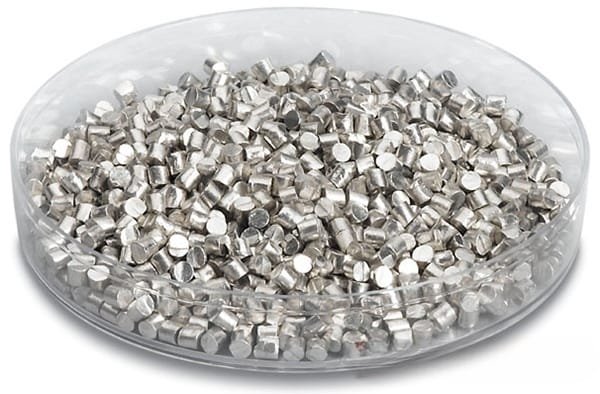
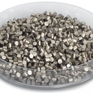
Available forms include:
Pieces or chunks
Granules
Pellets
Custom-shaped feedstock
Because indium oxidizes mildly in air, materials are surface-cleaned and vacuum-sealed before shipment to preserve evaporation quality. During deposition, indium demonstrates smooth melting behavior, which supports uniform film thickness and reproducible coating performance.
Indium is also widely used as a precursor for indium oxide (In₂O₃) films or in combination with tin to produce indium tin oxide (ITO), a key transparent conducting material.
Applications
Indium Evaporation Materials are widely used in:
Transparent conductive oxide (TCO) film deposition
Indium oxide (In₂O₃) thin films
Indium tin oxide (ITO) coatings
Infrared detector fabrication
III–V compound semiconductor growth
LED and display technologies
Soldering and bonding layers
Thin film photovoltaic research
In advanced semiconductor manufacturing, indium layers are often used as buffer layers, conductive films, or alloying components.
Technical Parameters
| Parameter | Typical Value / Range | Importance |
|---|---|---|
| Material | Indium (In) | Functional thin film source |
| Purity | 99.99% – 99.999% (4N–5N) | Reduces film impurities |
| Form | Pieces / Granules / Pellets | Compatible with evaporation systems |
| Melting Point | 156.6°C | Low thermal load deposition |
| Boiling Point | 2072°C | Suitable vapor pressure control |
| Deposition Method | E-beam / Thermal Evaporation | Flexible process options |
Comparison with Related Materials
| Material | Key Advantage | Typical Application |
|---|---|---|
| Indium (In) | Low melting point & good conductivity | Conductive thin films |
| Indium Oxide | Transparent semiconductor | Display & photovoltaic coatings |
| ITO | High transparency + conductivity | Touch panels & displays |
| Gallium (Ga) | Semiconductor alloy component | Compound semiconductors |
Compared with gallium, indium offers better stability in metallic film form. Compared with indium oxide, pure indium provides greater flexibility for reactive or alloy-based deposition processes.
FAQ
| Question | Answer |
|---|---|
| Is indium suitable for thermal evaporation? | Yes, its low melting point makes it ideal for thermal evaporation systems. |
| Can ultra-high purity grades be supplied? | Yes, 4N to 5N purity levels are available for semiconductor applications. |
| Does indium oxidize easily? | A thin surface oxide may form in air, but this does not significantly affect evaporation performance. |
| Can customized shapes be provided? | Yes, material form can be tailored to specific crucible or source requirements. |
| How is it packaged? | Vacuum-sealed packaging prevents contamination and moisture exposure during shipment. |
Packaging
Our Indium Evaporation Materials (In) are meticulously tagged and labeled externally to ensure efficient identification and maintain high standards of quality control. Each batch is carefully packaged to prevent oxidation and mechanical damage during storage and transportation.
Conclusion
Indium Evaporation Materials (In) provide a reliable and high-purity solution for semiconductor thin film deposition, transparent conductive coatings, and advanced optoelectronic applications. With stable evaporation characteristics, customizable forms, and semiconductor-grade purity, indium remains a cornerstone material in modern electronic and photonic industries.
For detailed specifications and a quotation, please contact us at sales@thinfilmmaterials.com.


Reviews
There are no reviews yet.