Introduction
Bismuth Ferrite (Garnet) Evaporation Materials (Bi₃Fe₅O₁₂) are specialized ceramic materials used for the fabrication of advanced magnetic and magneto-optical thin films. As a garnet-structured ferrite compound, Bi₃Fe₅O₁₂ exhibits unique magnetic ordering, optical activity, and chemical stability, making it highly valuable for research in spintronics, photonics, and multifunctional oxide electronics.
In vacuum deposition processes such as electron-beam evaporation and thermal evaporation, Bi₃Fe₅O₁₂ evaporation materials are vaporized under high vacuum and deposited onto substrates to form thin films with controlled composition and crystal structure. These films are widely investigated in magneto-optical devices, magnetic sensors, and optical communication technologies where garnet-type materials provide exceptional performance.
Detailed Description
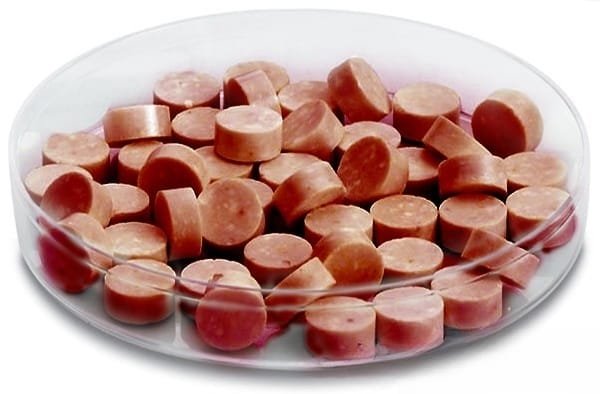
Bismuth Ferrite (Garnet) Evaporation Materials are typically produced using high-purity precursor oxides through controlled ceramic synthesis techniques such as solid-state reaction, calcination, and sintering. The resulting material is processed into pellets, granules, or evaporation charges suitable for vacuum deposition systems.
Bi₃Fe₅O₁₂ belongs to the garnet crystal family, which is well known for its magneto-optical properties. Garnet ferrites exhibit strong magnetic ordering and can interact with polarized light, making them useful for devices that rely on magneto-optical effects such as the Faraday rotation.
During deposition, Bi₃Fe₅O₁₂ evaporation materials are commonly used in electron-beam evaporation systems, which provide the energy necessary to evaporate complex oxide materials with relatively high melting temperatures. The e-beam method allows precise control of evaporation rate, film thickness, and deposition uniformity.
Thin films produced from Bi₃Fe₅O₁₂ evaporation materials can exhibit several valuable properties:
strong magneto-optical response
stable magnetic behavior
high chemical stability
compatibility with oxide substrates
good thermal stability
These properties make Bi₃Fe₅O₁₂ thin films suitable for experimental photonic and spintronic devices as well as advanced magnetic materials research.
Evaporation materials are typically supplied in granules, pellets, or irregular pieces that are compatible with standard evaporation crucibles and electron-beam sources used in thin film deposition systems.
Applications
Thin films deposited from Bi₃Fe₅O₁₂ Evaporation Materials are used in several advanced technological and research fields:
Magneto-optical devices – thin films used in optical isolators and optical modulators.
Spintronic materials research – garnet-based magnetic thin films for spin transport studies.
Optical communication components – magneto-optical materials for signal control and isolation.
Magnetic sensors – oxide thin films used in sensing technologies.
Photonic materials research – garnet thin films used in experimental photonic devices.
Academic and industrial R&D – multifunctional oxide thin film studies.
Technical Parameters
| Parameter | Typical Value / Range | Importance |
|---|---|---|
| Purity | 99.9% – 99.99% | High purity improves magnetic and optical film quality |
| Form | Pellets / Granules / Pieces | Compatible with evaporation sources |
| Particle Size | 1 – 6 mm typical | Ensures stable evaporation and material utilization |
| Deposition Method | Thermal or E-beam evaporation | Suitable for oxide thin film formation |
| Density | ≥95% theoretical | Improves evaporation stability |
Comparison with Related Materials
| Material | Key Advantage | Typical Application |
|---|---|---|
| Bi₃Fe₅O₁₂ (Bismuth Ferrite Garnet) | Strong magneto-optical properties | Photonic and spintronic devices |
| Yttrium Iron Garnet (Y₃Fe₅O₁₂) | Excellent magnetic characteristics | Microwave and magnetic devices |
| Bismuth Iron Oxide (BiFeO₃) | Multiferroic properties | Ferroelectric and spintronic materials |
FAQ
| Question | Answer |
|---|---|
| Can Bi₃Fe₅O₁₂ evaporation materials be customized? | Yes, particle size, purity, and packaging quantities can be customized according to deposition system requirements. |
| Which evaporation method is recommended for Bi₃Fe₅O₁₂? | Electron-beam evaporation is commonly used because it provides sufficient energy to evaporate complex oxide materials. |
| What substrates are typically used for Bi₃Fe₅O₁₂ thin films? | Silicon wafers, sapphire, glass, and oxide substrates are commonly used for magnetic oxide thin film research. |
| Are these materials used in magneto-optical research? | Yes, garnet ferrites such as Bi₃Fe₅O₁₂ are widely studied for magneto-optical devices and photonic technologies. |
| Which industries commonly use these materials? | Photonics research laboratories, semiconductor R&D facilities, and materials science institutes frequently use Bi₃Fe₅O₁₂ evaporation materials. |
Packaging
Our Bismuth Ferrite (Garnet) Evaporation Materials are meticulously tagged and labeled externally to ensure efficient identification and maintain high standards of quality control. Each batch is carefully vacuum-sealed and packaged with protective cushioning to prevent contamination or mechanical damage during storage and transportation. Export-grade cartons or wooden crates are used for secure international shipping.
Conclusion
Bismuth Ferrite (Garnet) Evaporation Materials (Bi₃Fe₅O₁₂) are advanced ceramic deposition materials used to produce high-performance magnetic and magneto-optical thin films. Their unique garnet crystal structure and magnetic behavior make them valuable for research in spintronics, photonics, and multifunctional oxide electronics.
With high purity, stable evaporation characteristics, and customizable forms, Bi₃Fe₅O₁₂ evaporation materials provide reliable performance for laboratories and industrial thin film deposition systems.
For detailed specifications and a quotation, please contact us at sales@thinfilmmaterials.com.


 MSDS File


Reviews
There are no reviews yet.